Date created: Monday, June 5, 2017 4:32:51 PM. Last modified: Friday, July 15, 2022 12:59:31 PM
MX Series Forwarding Hardware
References:
Juniper MX Series - https://www.safaribooksonline.com/library/view/juniper-mx-series/9781491932711/ch01.html
Juniper MX Series (2nd Edition) - http://shop.oreilly.com/product/0636920042709.do
Junos Networking Technologies - THIS WEEK: AN EXPERT PACKET WALKTHROUGH ON THE MX SERIES 3D
https://en.wikipedia.org/wiki/Application-specific_instruction_set_processor
https://www.juniper.net/documentation/en_US/release-independent/junos/topics/reference/general/mpc-mx-series-supported.html
https://kb.juniper.net/InfoCenter/index?page=content&id=KB23065&actp=METADATA
Contents:
Trio Overview
Buffering Block
Lookup Block
Interfaces Block
Dense Queuing Block
DPC Line Cards
MPC Features and Scaling
MPC1
MPC2
A Note on HSL2, UPOH and MAC Mode
MPC3
NG-MPC2E/3E
MPC4
MPC5
MPC6
MPC7
MPC8
MPC9
Multiple Lookup Block Architecture
Switch Control Boards and Switch Fabric
Line Card and RE CPU Paths
Fabric Queuing, Grants and Mixing DCPE with MPC
MPC1 and MPC2 Ingress Packet Walkthrough
MPC1 and MPC2 Egress Packet Walkthrough
MPC3 Ingress Packet Walkthrough
MPC3 Egress Packet Walkthrough
Life of Packet inside Trio 6
Trio Overview
The Juniper Trio chipset is built upon a Network Instruction Set Processor (NISP) which is an Application-Specific Instruction set-Processor (ASIP). The instruction set of an ASIP is tailored to benefit a specific application (in this case, packet processing). This specialization of the NISP/ASIP core provides a trade-off between the flexibility of a general purpose CPU and the performance of an ASIC. Trio has the performance of a traditional ASIC, but the flexibility of a field-programmable gate array (FPGA) by allowing the installation of new features via software. This Trio chipset/PFE (these two terms are used interchangeably) also contains lookup memory and packet buffers and overall forms an NPU (Network Processor Unit).
Some of the tasks that can be offloaded to a Trio NPU include:
- Tunnel encapsulation and decapsulation
- IP Flow Information Export
- Network Address Translation
- Bidirectional Forwarding Detection
- Ethernet operations, administration, and management
- Instantaneous Link Aggregation Group convergence
The Trio chipset comprises of four major building blocks: Buffering, Lookup, Interfaces, and Dense Queuing. "As new MICs are released, they may or may not have an Interfaces Block depending on power requirements and other factors. Remember that the Trio function blocks are like building blocks and some blocks aren't required to operate." The Trio chipset is also referred to in Junos terminology as the PFE (Packet Forwarding Engine) and is a set of ASICs and NISPs. "Some of them [the ASICs] are embedded on all types of MPCs while others are optional and are only available on certain MPC models...The Enhanced CoS and Interface Adaptation ASICs are optional and are not included in all MPC/MIC models. Inversely, Routing and Forwarding ASICs are always present and constitute the core of an MPC's Packet Forwarding Engine (PFE)." – This means that all the line cards support "distributed forwarding" like with Cisco ASR9000 line cards for example, and unlike Cisco 7600 or 6500 cards when using CFCs (cards without a DFC) which rely on the PFC for central forwarding decisions.
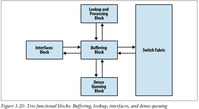
Buffering Block
The Buffering Block ties together all of the other functional Trio blocks. It primarily manages packet data, fabric queuing, and revenue port queuing. The Buffering Block is able to process basic per port queuing. Each port has eight hardware queues, large delay buffers, and low latency queues (LLQs). If there's a requirement to have hierarchical class of service (H-QoS) and additional scale, this functionality can be delegated to the Dense Queuing Block.
The "Buffering Block" uses the MQ chip (Memory and Queuing) inside the PFE on MPC Type 1 and 2. On MPC3E cards the XM chip (or "XMq" for "enhanced") is the Buffering Block. The XM provides the same functionalities as MQ but with new features and scaling four times more than MQ. XM load balances the traffic towards four LU chips. Also The MPC3E's XM chip doesn't directly connect to the fabric planes, instead one XF ASIC, programmed in Fabric Offload mode plays the role of gateway between the PFE and the fabric. This is the same XF ASIC that you'll find in SCBE cards, although on SCBEs the XF is programed in Standalone mode instead. In the MPC3E this chip just provides compatibility with legacy fabric chips of the original SCB model. In the MPC4E cards the XM chip is directly connected to the fabric planes.
Lookup Block
The Lookup Block has multi-core processors to support parallel tasks using multiple threads. The Lookup Block supports all of the packet header processing such as:
- Route lookups
- MAC lookups
- Class of Service (QoS) Classification
- Firewall filters
- Policers
- Accounting
- Encapsulation
- Statistics
- Load-balancing
- Inline ppmd (e.g. BFD)
A key feature in the Lookup Block is that it supports Deep Packet Inspection (DPI) and is able to look over 256 bytes into the packet. As packets are received by the Buffering Block, the packet headers are sent to the Lookup Block for additional processing. All processing is completed in one pass through the Lookup Block regardless of the complexity of the workflow. Once the Lookup Block has finished processing, it sends the modified packet headers back to the Buffering Block to send the packet to its final destination. In order to process data at line rate, the Lookup Block has a large bucket of reduced-latency dynamic random access memory (RLDRAM) that is essential for packet processing. The "Lookup Block" is the LU chip inside the PFE on MPC1 and MPC2 cards.
Interfaces Block
One of the optional components is the Interfaces Block. Its primary responsibility is to intelligently handle oversubscription. When using a MIC that supports less than 24x1GE or 2x10GE MACs, the Interfaces Block is used to manage the oversubscription.
Each packet is inspected at line rate and attributes are used to evaluate which buffers to enqueue the packet towards the Buffering Block. Pre-classification allows the ability to drop excess packets as close to the source as possible, while allowing critical control plane packets through to the Buffering Block.
There are four queues between the Interfaces and Buffering Block: real-time, control traffic, best effort, and packet drop. Currently, these queues and pre-classifications are not user configurable; however, it's possible to take a peek at them.
$ request pfe execute target fpc1 command "show precl-eng summary"
$ request pfe execute target fpc1 command "show precl-eng 1 statistics"
The output will show "IX_engine" with MICs that support an Interfaces Block. MICs such as the 4x10GE do not have an Interfaces Block, so the pre-classification is performed on the Buffering Block and the command output would show "MQ_engine." The "Interface Block" is the IX chip on MPC1 and MPC2 PFEs.
Dense Queuing Block
Depending on the line card, Trio offers an optional Dense Queuing Block that offers rich Hierarchical QoS that supports up to 512,000 queues. The Dense Queuing Block is an optional functional Trio block. The Buffering Block already supports basic per port queuing. The Dense Queuing Block is only used in line cards that require H-QoS or additional scale beyond the Buffering Block. The "Dense Queueing Block" is the QX chip on MPC2 line cards.
DPC Line Cards
A Flexible Port Concentrator (FPC) called the Dense Port Concentrator (DPC) was the first-generation line card for the MX series and it allowed up to 80Gbps ports per slot. The DPC line cards utilize a previous ASIC/NPU from the Juniper M series routers called the I-CHIP (version 3). The DPC line cards come in six different models to support varying different port configurations. There's a mixture of 1G, 10G, copper, and optical. There are three DPC types: routing and switching (DPCE-R), switching (DPCE-X), and enhanced queuing (DPCE-Q).
Output from MX480 with DCP cards:

> show chassis hardware
Item Version Part number Serial number Description
...
FPC 0 REV 14 750-017679 XXXXXX DPCE 20x 1GE R EQ
CPU REV 03 710-022351 XXXXXX DPC PMB
PIC 0 BUILTIN BUILTIN 10x 1GE(LAN) EQ
PIC 1 BUILTIN BUILTIN 10x 1GE(LAN) EQ
> request pfe execute command "show jspec client" target fpc0
SENT: Ukern command: show jspec client
GOT: ID Name
GOT: 1 IA_0
GOT: 2 ichip_0
GOT: 3 IA_1
GOT: 4 ichip_2
MPC Features and Scaling
As of Junos 14.2 there are twelve different models/categories of MPCs. Each model has a different number of Trio PFEs providing different options for scaling and bandwidth:
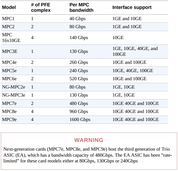
MPC line cards support the ability to operate in Layer 2, Layer 3, or Enhanced Queuing modes.
The MX-3D has the same features and services as the MX-3D-R-B but with limited Layer 3 scaling. When using BGP or an IGP, the routing table is limited to 32,000 routes. The other restriction is that MPLS L3VPNs cannot be used on these line cards.
The MX-3D-Q has the same features, services, and reduced Layer 3 capacity as the MX-3D, but with Enhanced Queuing.
The MX-3D-R-B supports full Layer 3 and Layer 2 switching support.
The MX-3D-Q-R-B combines all of the features together to offer full Layer 2, Layer 3, and Enhanced Queuing together in one line card.
MPC1
The Modular Port Concentrator (MPC) is the second-generation FPC created to further increase the throughput per slot. This generation of hardware is created using the Trio chipset. The MPC supports MICs that allow you to mix and match different modules on the same MPC or fixed port configurations.
The MPC1 has one Junos Trio chipset (PFE) and supports 40Gbps full-duplex throughput. The MPC1 has two MIC slots. All of the MICs that are compatible with the MPC1 have the Interfaces Block built into the MIC to handle oversubscription:
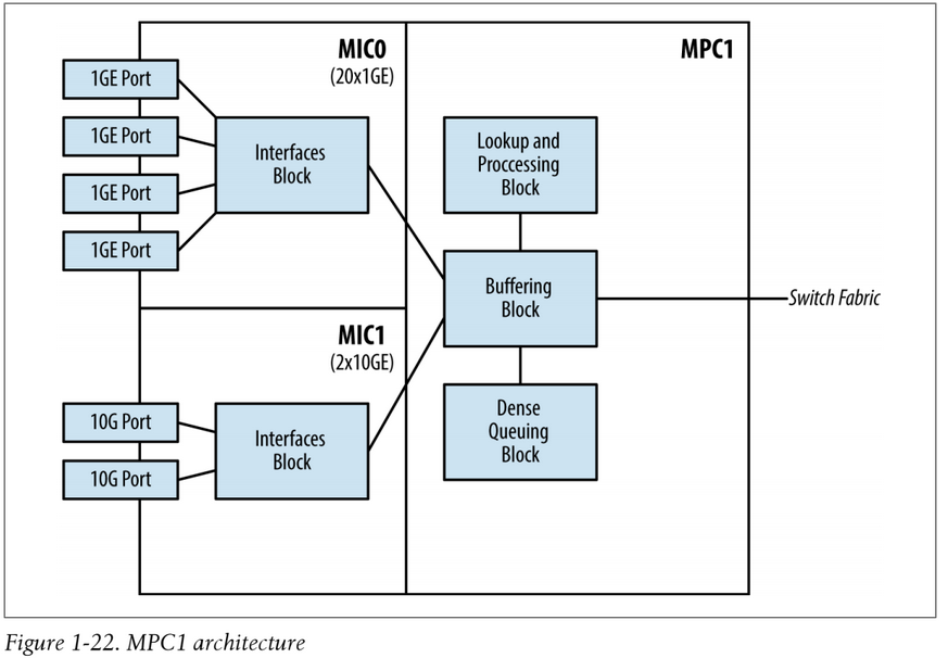
With the MPC1, the single Trio chipset handles both MICs. Each MIC is required to share the bandwidth that's provided by the single Trio chipset, thus the Interfaces Block is delegated to each MIC to intelligently handle oversubscription. Because each Trio chipset can only operate in MAC mode or UPOH mode, the MPC1 must operate in MAC mode to be able to support the 20x1GE and 2x10GE MICs. Unfortunately, the 4x10GE MIC only operates in UPOH mode and isn't compatible with the MPC1.
This diagram shows an MPC1 with two MIC cards, one MIC card has an IX chip (an example of a MIC with oversubscription) and the other doesn't, but both MICs use the single Trio chipset on the MPC1 for basic buffering (note the Memory and Queueing chip) and forwarding lookups (note the LU chip):
MPC2
The MPC2 is similar in architecture to the MPC1 but with two Trio chipsets supporting up to 80Gbps full-duplex. The MPC2 has two MIC slots. In example MPC2 the diagram below it can be seen that a 20x1G card is in MIC0 and a 4x10G card in MIC1, note the interface block (IX chip) in the 20x1G card, this means PFE0 (for MIC0) is operating in MAC mode and PFE1 (for MIC1) is operating in UPOH mode (this will be explained further down):
The MPC2 offers a dedicated Trio chipset per MIC, effectively doubling the bandwidth and scaling from the previous MPC1. The MPC2 is able to operate in both MAC mode and UPOH mode. Actually the Trio chipset used in the MPC1s and MPC2s have slightly less than 40Gbps throughput full-duplex as a single Trio chipset has a little over 70Gbps of memory bandwidth, so 40Gbps of traffic coming into an MPC1 or MPC2 Trio means that only about 30-something-Gbps can leave the Trio.
The diagram below shows an MPC2 card which supports two MICs and has one PFE per MIC (just one MIC and PFE is shown below, note the QX chip is the "Dense Queuing Block" and MQ chip is the "Buffering Block"):
Not all MPC cards take MIC cards, some are fixed port configuration MPCs. For example the MPC-3D-16XGE-SFPP line card is a fixed port 16x 10Gig SFP+ configuration with one Junos Trio chipset per set of four ports (4 Trios in total providing about 70Gbps of throughput per 4x10G port group), but only uses the Buffering Block and Lookup Block in the PFE complex. Also an SCBE fabric module would be required for the full 160Gbps of throughput as opposed to an SCB.
In the output below it can be seen that an MX-MPC2E-3D-Q Modular Port Concentrator is present, which has two PFEs (one per MIC slot), MIC0 contains Modular Interface Card MIC-3D-4XGE-XFP and MIC1 contains MIC-3D-2XGE-XFP.
Output from MX480 with MPC2E:

> show chassis hardware
Item             Version  Part number  Serial number     Description
…
FPC 0            REV 09   750-038493   XXXXXXXX          MPCE Type 2 3D Q
  CPU            REV 04   711-038484   XXXXXXXX          MPCE PMB 2G
  MIC 0          REV 30   750-028387   XXXXXXXX          3D 4x 10GE  XFP
    PIC 0                 BUILTIN      BUILTIN           2x 10GE  XFP
      Xcvr 0     REV 01   740-011607   XXXXXXXXXXXX      XFP-10G-LR
      Xcvr 1     REV 01   740-031833   XXXXXXXXXXXX      XFP-10G-LR
    PIC 1                 BUILTIN      BUILTIN           2x 10GE  XFP
      Xcvr 0     REV 01   740-031833   XXXXXXXXXXXX      XFP-10G-LR
      Xcvr 1     REV 01   740-031833   XXXXXXX           XFP-10G-LR
  MIC 1          REV 21   750-028380   XXXXXXXX          3D 2x 10GE XFP
    PIC 2                 BUILTIN      BUILTIN           1x 10GE XFP
      Xcvr 0     REV 01   740-031833   XXXXXXX           XFP-10G-LR
    PIC 3                 BUILTIN      BUILTIN           1x 10GE XFP
      Xcvr 0     REV 01   740-031833   XXXXXXXXXXXX      XFP-10G-LR
  QXM 0          REV 06   711-028408   XXXXXXXX          MPC QXM
  QXM 1          REV 06   711-028408   XXXXXXXX          MPC QXM
In the output below it can be seen that each PFE inside the MPC2E-3D-Q card has an LU chip, an MQ chip and also a QX chip (note the –Q in the card name for "enhanced queueing). Note there is one IX chip present also, this is on the MIC-3D-2XGE-XFP card (explained below).
Output from MX240 with MPC2E
> request pfe execute command "show jspec client" target fpc0
SENT: Ukern command: show jspec client
GOT:  ID       Name
GOT:   1       LUCHIP[0]
GOT:   2       QXCHIP[0]
GOT:   3       MQCHIP[0]
GOT:   4       LUCHIP[1]
GOT:   5       QXCHIP[1]
GOT:   6       MQCHIP[1]
GOT:   7       IXCHIP[2]
LOCAL: End of file
The outputs below from an MX104 show that it has what it calls AFEB0, because it's a fixed chassis device (with some MIC slots). It is a fixed fabric which is some kind of MPC2 (MX80's have TFEB0 which is also a kind of fixed MPC1). The outputs shows that the MX104 has 20x1GE fixed MIC inserted and the 4x10GE built in ports:
user@lab104> show chassis hardware
Hardware inventory:
Item             Version  Part number  Serial number     Description
Chassis                                XXXXX             MX104
Midplane         REV 56   750-062050   XXXXXXXX          MX104
PEM 0            REV 05   740-045933   XXXXXXXXXXX       AC Power Entry Module
PEM 1            REV 05   740-045933   XXXXXXXXXXX       AC Power Entry Module
Routing Engine 0 REV 04   750-061985   XXXXXXXX          RE-MX-104
Routing Engine 1 REV 04   750-061985   XXXXXXXX          RE-MX-104
AFEB 0                    BUILTIN      BUILTIN           Forwarding Engine Processor
FPC 0                     BUILTIN      BUILTIN           MPC BUILTIN
  MIC 0          REV 36   750-028392   XXXXXXXX          3D 20x 1GE(LAN) SFP
    PIC 0                 BUILTIN      BUILTIN           10x 1GE(LAN) SFP
      Xcvr 0     REV 02   740-013111   XXXXXXX           SFP-T
      Xcvr 1     REV 01   740-038291   XXXXXXX           SFP-T
      Xcvr 2     REV 02   740-011613   XXXXXXXXXXX       SFP-SX
      Xcvr 3     REV 01   740-011614   XXXXXXXXXXX       SFP-LX10
      Xcvr 8     REV 01   740-038291   XXXXXXX           SFP-T
      Xcvr 9              NON-JNPR     XXXXXXXXXXX       SFP-T
    PIC 1                 BUILTIN      BUILTIN           10x 1GE(LAN) SFP
FPC 1                     BUILTIN      BUILTIN           MPC BUILTIN
FPC 2                     BUILTIN      BUILTIN           MPC BUILTIN
  MIC 0                   BUILTIN      BUILTIN           4x 10GE(LAN) SFP+
    PIC 0                 BUILTIN      BUILTIN           4x 10GE(LAN) SFP+
Fan Tray 0       REV 03   711-049570   XXXXXXXX          Fan Tray

user@lab104> show chassis hardware models
Hardware inventory:
Item             Version  Part number  Serial number     FRU model number
Midplane         REV 56   750-062050   XXXXXXXX          CHAS-MX104-S
PEM 0            REV 05   740-045933   XXXXXXXXXXX       PWR-MX104-AC-S
PEM 1            REV 05   740-045933   XXXXXXXXXXX       PWR-MX104-AC-S
Routing Engine 0 REV 04   750-061985   XXXXXXXX          RE-S-MX104-S
Routing Engine 1 REV 04   750-061985   XXXXXXXX          RE-S-MX104-S
AFEB 0                    BUILTIN      BUILTIN
FPC 0                     BUILTIN      BUILTIN
  MIC 0          REV 36   750-028392   XXXXXXXX          MIC-3D-20GE-SFP
FPC 1                     BUILTIN      BUILTIN
FPC 2                     BUILTIN      BUILTIN
Fan Tray 0       REV 03   711-049570   XXXXXXXX          FANTRAY-MX104-S
It can also be seen below that the MX104 AFEB has one of each chip: LUCHIP, QXCHIP, MQCHIP and IXCHIP. One LUCHIP means the forwarding capacity is similar to an MPC2):
user@lab104> request pfe execute target afeb0 command "show jspec client"
================ afeb0 ================
SENT: Ukern command: show jspec client

 ID       Name
  1       LUCHIP[0]
  2       QXCHIP[0]
  3       MQCHIP[0]
  4       IXCHIP[0]
The MQ chip on the MPC2 Trio chipset can communicate directly with the PHY on the 4x10G card, in the MPC1 cards the Trio chipset could not do this and the 2x10G card has an IX chip present in-between PHY and MQ. This means the 4x10G card is not supported in MPC1 FPCs but the 2x10G card is (even further explanation below in the section on HSL2 section).
The diagrams below show the MPC2 MPC-3D-16XGE-SFPP card, it has no MICs and four PFEs, one per each group of 4x 10GBE ports:
A Note on HSL2, UPOH and MAC Mode
High Speed Link Version 2 is a physical link technology that makes it possible to convey high speed data among ASICs in a same PFE but also between PFEs and the fabric (this is how the forwarding plane is actually implemented: every transit packet spends some time through HSL2 links). The data layer protocol over HSL2 allows channelization and supports error detection via a CRC mechanism. Once can retrieve HSL2 links and their statistics by using the following microkernel shell command: "request pfe execute target fpc0 command "show hsl2 statistics"
The Buffering Block's WAN interface can operate either in MAC mode or in the Universal Packet over HSL2 (UPOH) mode. This creates a difference in operation between the MPC1 and MPC2 line cards. The MPC1 only has a single Trio chipset, the single Trio chipset handles both MICs and thus only MICs that can operate in MAC mode are compatible with this line card. Each MIC is required to share the bandwidth that's provided by the single Trio chipset, thus the Interfaces Block is delegated to each MIC to intelligently handle oversubscription. This is because each Trio chipset can only operate in MAC mode or UPOH mode, the MPC1 must operate in MAC mode to be able to support the 20x1GE and 2x10GE MICs. On the other hand, the MPC2 has two Trio chipsets. Each MIC on the MPC2 is able to operate in either mode, thus compatible with more MICs. This means, for example, that the 4x10GE MIC only operates in UPOH mode and thus isn't compatible with the MPC1.
MPC3
The MPC3E is the first modular line card for the MX Series to accept 100G and 40G MICs. The MPC3Es have one enhanced Junos Trio chipset and supports up to 130Gbps of full duplex throughput (to accommodate a 100Gbps interface). The MPC3Es have two MIC slots.
The main MPC3E enhancements are that the Buffering Block has been increased to support 130Gbps throughput (using the XM chip over the MQ chip) and the number of Lookup Blocks has been increased to four in order to support 100GE interfaces. Also the fabric switching functionality has been moved out of the Buffering Block and into a new Fabric Functional Block (the XF chip). The MPC3E can provide line-rate performance for a single 100GE interface. The MPC3E can support 2x100GE interfaces but the Buffering Block limitation means it is oversubscribed 200:130, or roughly 1.5:1. Enhanced Queuing isn't supported on the MPC3E due to the lack of a Dense Queuing Block. However, this doesn't mean that the MPC3E isn't capable of class of service. The Buffering Block, just like the MPC-3D-16x10GE-SFPP, is capable of basic port-level class of service.
The first generation of MPCs, containing the original Trio chipset with LU and MQ chips includes MPC types 1 and 2, as well as the MPC 16x10GE. The Second generation of MPCs who's PFEs have LU and XM chips include MPC3E and MPC4E cards. The third generation of MPCs who's PFEs have XL, XQ, and XM chips includes MPC5E and MPC6E cards.
Some example MPC3 MIC cards include:
- MIC3-3D-1X100GE-CFP (1x100GE)
- MIC3-3D-1X100GE-CXP (1x100GE)
- MIC3-3D-10XGE-SFPP (10x10GE)
- MIC3-3D-2X40GE-QSFP (2x40GE)
- MIC-3D-20GE-SFP (20x1GE)
- MIC-3D-2XGE-XFP (2x10GE)
The diagram below shows an MPC3E card with two MIC slots and one Enhanced Trio chipset (note four LU chips and one XM chip instead of an MQ chip):
NG-MPC2E/3E
The NG-MPC2 and NG-MPC3E linecards both use the set of ASICs (XL+XM+XQ) which means that the two types of card have exactly the same hardware architecture. The only difference is that the PFE is clocked higher on the NG-MPC3E. The NG-MPC2E has 80Gbps of bandwidth while the PFE of the NG-MPC3E has 130Gbps of bandwidth. Both MPCs are implemented around one PFE made from one XL chip, one XM chip, and optionally "Q-" versions of cards have the XQ chip also.
The below output is from an MX960 which has an MPC2E-NG in FPC0 and MPC3E-NG in FPC2:
NGMPC0(THE-STAGING vty)# show hsl2 asic

   XL[0:0](42)  16 channels  1 serdes 192 links  chip_flag 0x40000009
 XMCHIP(0)(32)  142 channels 10 serdes 204 links  chip_flag 0x40000009
   PFE0_XF(40)  480 channels 32 serdes 256 links  chip_flag 0x9
 IXCHIP(0)(20)   6 channels  2 serdes  16 links  chip_flag 0x40000009

NGMPC2(THE-STAGING vty)# show hsl2 asic

   XL[0:0](42)  16 channels  1 serdes 192 links  chip_flag 0x40000009
 XMCHIP(0)(32)  142 channels 10 serdes 204 links  chip_flag 0x40000009
   PFE0_XF(40)  480 channels 32 serdes 256 links  chip_flag 0x9
The below output is from an MX480 with MPC2E-NG and MPC3E-NG cards present and shows a difference in ASICs on the PFEs:
user@lab480> show chassis hardware
Hardware inventory:
Item             Version  Part number  Serial number     Description
Chassis                                XXXXXXXXXXXX      MX480
Midplane         REV 05   710-017414   XXXXXXXX          MX480 Midplane
FPM Board        REV 02   710-017254   XXXXXXXX          Front Panel Display
PEM 0            Rev 09   740-029970   XXXXXXXXXXX       PS 1.4-2.52kW; 90-264V AC in
PEM 1            Rev 09   740-029970   XXXXXXXXXXXX      PS 1.4-2.52kW; 90-264V AC in
PEM 2            Rev 09   740-029970   XXXXXXXXXXXX      PS 1.4-2.52kW; 90-264V AC in
PEM 3            Rev 09   740-029970   XXXXXXXXXXXX      PS 1.4-2.52kW; 90-264V AC in
Routing Engine 0 REV 16   750-054758   XXXXXXXX          RE-S-2X00x6
CB 0             REV 09   750-062572   XXXXXXXX          Enhanced MX SCB 2
CB 1             REV 09   750-062572   XXXXXXXX          Enhanced MX SCB 2
FPC 0            REV 09   750-038493   XXXXXXXX          MPCE Type 2 3D Q
  CPU            REV 04   711-038484   XXXXXXXX          MPCE PMB 2G
  MIC 0          REV 30   750-028387   XXXXXXXX          3D 4x 10GE  XFP
    PIC 0                 BUILTIN      BUILTIN           2x 10GE  XFP
      Xcvr 0     REV 01   740-011607   XXXXXXXXXXXX      XFP-10G-LR
      Xcvr 1     REV 01   740-031833   XXXXXXXXXXXX      XFP-10G-LR
    PIC 1                 BUILTIN      BUILTIN           2x 10GE  XFP
      Xcvr 0     REV 01   740-031833   XXXXXXXXXXXX      XFP-10G-LR
      Xcvr 1     REV 01   740-031833   XXXXXXX           XFP-10G-LR
  MIC 1          REV 21   750-028380   XXXXXXXX          3D 2x 10GE XFP
    PIC 2                 BUILTIN      BUILTIN           1x 10GE XFP
      Xcvr 0     REV 01   740-031833   XXXXXXX           XFP-10G-LR
    PIC 3                 BUILTIN      BUILTIN           1x 10GE XFP
      Xcvr 0     REV 01   740-031833   XXXXXXXXXXXX      XFP-10G-LR
  QXM 0          REV 06   711-028408   XXXXXXXX          MPC QXM
  QXM 1          REV 06   711-028408   XXXXXXXX          MPC QXM
FPC 1            REV 09   750-038493   XXXXXXXX          MPCE Type 2 3D Q
  CPU            REV 04   711-038484   XXXXXXXX          MPCE PMB 2G
  MIC 0          REV 21   750-028380   XXXXXXXX          3D 2x 10GE XFP
    PIC 0                 BUILTIN      BUILTIN           1x 10GE XFP
      Xcvr 0     REV 01   740-031833   XXXXXXXXXXXX      XFP-10G-LR
    PIC 1                 BUILTIN      BUILTIN           1x 10GE XFP
      Xcvr 0     REV 01   740-033777   XXXXXXX           XFP-10G-SR
  QXM 0          REV 06   711-028408   XXXXXXXX          MPC QXM
  QXM 1          REV 06   711-028408   XXXXXXXX          MPC QXM
FPC 5            REV 11   750-063180   XXXXXXXX          MPC3E NG HQoS
  CPU            REV 13   711-045719   XXXXXXXX          RMPC PMB
  MIC 0          REV 14   750-033307   XXXXXXXX          10X10GE SFPP
    PIC 0                 BUILTIN      BUILTIN           10X10GE SFPP
      Xcvr 0     REV 01   740-021309   XXXXXXXXXX        SFP+-10G-LR
      Xcvr 1     REV 01   740-021309   XXXXXXXXXX        SFP+-10G-LR
      Xcvr 8     REV 01   740-021309   XXXXXXXXXX        SFP+-10G-LR
      Xcvr 9     REV 01   740-021309   XXXXXXXXXX        SFP+-10G-LR
  MIC 1          REV 16   750-036233   XXXXXXXX          2X40GE QSFPP
    PIC 2                 BUILTIN      BUILTIN           2X40GE QSFPP
      Xcvr 0     REV 01   740-032986   XXXXXXXX          QSFP+-40G-SR4
Fan Tray                                                 Enhanced Left Fan Tray


user@lab480> show chassis hardware models
Hardware inventory:
Item             Version  Part number  Serial number     FRU model number
Midplane         REV 05   710-017414   XXXXXXXX          CHAS-BP-MX480-S
FPM Board        REV 02   710-017254   XXXXXXXX          CRAFT-MX480-S
PEM 0            Rev 09   740-029970   XXXXXXXXXXX       PWR-MX480-2520-AC-S
PEM 1            Rev 09   740-029970   XXXXXXXXXXX       PWR-MX480-2520-AC-S
PEM 2            Rev 09   740-029970   XXXXXXXXXXX       PWR-MX480-2520-AC-S
PEM 3            Rev 09   740-029970   XXXXXXXXXXX       PWR-MX480-2520-AC-S
Routing Engine 0 REV 16   750-054758   XXXXXXXX          RE-S-X6-64G-S
CB 0             REV 09   750-062572   XXXXXXXX          SCBE2-MX-S
CB 1             REV 09   750-062572   XXXXXXXX          SCBE2-MX-S
FPC 0            REV 09   750-038493   XXXXXXXX          MX-MPC2E-3D-Q
  MIC 0          REV 30   750-028387   XXXXXXXX          MIC-3D-4XGE-XFP
  MIC 1          REV 21   750-028380   XXXXXXXX          MIC-3D-2XGE-XFP
FPC 1            REV 09   750-038493   XXXXXXXX          MX-MPC2E-3D-Q
  MIC 0          REV 21   750-028380   XXXXXXXX          MIC-3D-2XGE-XFP
FPC 5            REV 11   750-063180   XXXXXXXX          MPC3E-3D-NG-Q
  MIC 0          REV 14   750-033307   XXXXXXXX          MIC3-3D-10XGE-SFPP
  MIC 1          REV 16   750-036233   XXXXXXXX          MIC3-3D-2X40GE-QSFPP
Fan Tray                                                 FFANTRAY-MX480-HC-S


user@lab480> request pfe execute target fpc0 command "show precl-eng summary"
SENT: Ukern command: show precl-eng summary

 ID  precl_eng name       FPC PIC   (ptr)
--- -------------------- ---- ---  --------
  1 MQ_engine.0.0.16       0   0  59149d48
  2 IX_engine.0.1.22       0   1  595352

user@lab480> request pfe execute target fpc0 command "show jspec client"
SENT: Ukern command: show jspec client


 ID       Name
  1       LUCHIP[0]
  2       QXCHIP[0]
  3       MQCHIP[0]
  4       LUCHIP[1]
  5       QXCHIP[1]
  6       MQCHIP[1]
  7       IXCHIP[2]


user@lab480> request pfe execute target fpc5 command "show precl-eng summary"
SENT: Ukern command: show precl-eng summary

 ID  precl_eng name       FPC PIC   (ptr)
--- -------------------- ---- ---  --------
  1 XM_engine.5.0.32       5   0  357a10d0
  2 XM_engine.5.1.65568    5   1  369ec4e0

SENT: Ukern command: show jspec client


 ID       Name
  1       MPCS[0]
  2       xfi2xaui[0]
  3       xfi2xaui[1]
  4       XR2CHIP[0]
  5       XR2CHIP[1]
  6       XR2CHIP[2]
  7       XLCHIP[0]
  8       XQCHIP[0]
  9       XMCHIP[0]
 10       PFE0_XF
MPC4
Fixed port line card examples include the MPC4E cards which offer fixed port configurations only. The MPC4E is a Trio based card which uses the same (130Gbps) enhanced version of the Trio used in the MPC3E cards. MPC4E-3D-32XGE-SFPP which is a fixed 32x 10Gig SFP+ port configuration that supports a line-rate throughput of up to 260Gbps (oversubscribed at 320:260) with an SCBE or full 320Gbps on SCBE2. The MPC4E-3D-2CGE-8XGE is a fixed 2x 100G and 8x 10G port card and supports line-rate throughput of up to 260Gbps (slightly oversubscribed at 280:260) on SCBE but full throughput on the SCBE2.
It can be seen in the diagram below of the MPC4E-3D-2CGE-8XGE card it has 2 PFEs and each PFE/Trio Chipset controls 1x 100G port and 4x 10G ports (note the single XM chip and two LU chips per PFE):
With the MPC4E 32x10GE card, PFE 0, WAN Group 0 is associated to the first 8x10GE ports and WAN Group 1 to the next eight ports. For PFE 1 this is the same for the remaining 16x10GE ports.
With the MPC4E 8x10GE+2x100GE card, PFE 0, WAN Group 0 is associated to the first 4x10GE ports and WAN Group 1 to the first 1x100GE port. For PFE 1 this is the same for the remaining 4x10GE and 1x100GE ports.
MPC5
The MPC5E cards are all fixed port configuration cards and support line-rate throughput of up to 240Gbps using a single 2nd Gen Trio packet-forwarding engine per line-card.
MPC5E cards include:
- MPC5E-40G10G (6x40GE and 24x10GE, 1:2 oversubscribed)
- MPC5EQ-40G10G (6x40GE and 24x10GE, dense queuing with XQ ASIC)
- MPC5E-100G10G (2x100GE and 4x10GE)
- MPC5EQ-100G10G (2x100GE and 4x10GE, dense queuing with XQ ASIC)
MPC6
The MX2K-MPC6E cards are modular cards and have two 240Gbps PFEs supporting a maximum rate of 480Gbps. These are for the MX2K series routers. The MPC6E has two MIC slots.
MPC6E MIC cards include:
- MX2K-MIC6-24XE (24x10GE)
- MX2K-MIC6-4CE-CXP (4x100GE)
- MX2K-MIC6-24XE-OTN (24x10G OTN)
- MX2K-MIC6-2CE-CFP2 (2x100G OTN)
- MIC6-10G: (24x10GE, no-oversubscription)
- MIC6-100G-CFP2: 2x100GE, no-oversubscription)
- MIC6-100G-CXP: (4x100GE, 1:2 oversubscription)
MPC7
The MPC7e is the first MPC based on the Trio EA ASIC. This MPC has a total bandwidth of 480Gbps and is made of two PFEs. Each PFE is actually made from one Eagle (EA) chip (The EA chip on the MPC7e is rate limited at 240Gbps).
The MPC7E MultiRate cards have mixed 10GE/40GE/100GE ports which supports different throughputs depending on the port combinations configure. This multi-rate cards supports up to 400Gbps on the MX240, MX480, MX960 and MX2000.
There is also a 40x10GE card which supports up to 400Gbps on MX240, MX480, MX960, MX2010, and MX2020 routers.
user@r1> show chassis hardware
Hardware inventory:
Item             Version  Part number  Serial number     Description
Chassis                                123456789012      MX480
Midplane         REV 09   750-047862   12345678          Enhanced MX480 Midplane
FPM Board        REV 02   710-017254   12345678          Front Panel Display
PEM 0            Rev 10   740-029970   12345678901       PS 1.4-2.52kW; 90-264V AC in
PEM 1            Rev 10   740-029970   12345678901       PS 1.4-2.52kW; 90-264V AC in
PEM 2            Rev 10   740-029970   12345678901       PS 1.4-2.52kW; 90-264V AC in
PEM 3            Rev 10   740-029970   12345678901       PS 1.4-2.52kW; 90-264V AC in
Routing Engine 0 REV 17   750-054758   12345678          RE-S-2X00x6
Routing Engine 1 REV 17   750-054758   12345678          RE-S-2X00x6
CB 0             REV 03   750-055976   12345678          Enhanced MX SCB 2
CB 1             REV 03   750-055976   12345678          Enhanced MX SCB 2
FPC 0            REV 47   750-056519   12345678          MPC7E 3D MRATE-12xQSFPP-XGE-XLGE-CGE
  CPU            REV 21   750-057177   12345678          SMPC PMB
  PIC 0                   BUILTIN      BUILTIN           MRATE-6xQSFPP-XGE-XLGE-CGE
    Xcvr 2       131 nm   740-058732   1234567           QSFP-100GBASE-LR4
    Xcvr 5       131 nm   740-058732   1234567           QSFP-100GBASE-LR4
  PIC 1                   BUILTIN      BUILTIN           MRATE-6xQSFPP-XGE-XLGE-CGE
    Xcvr 2       131 nm   740-058732   1234567           QSFP-100GBASE-LR4
    Xcvr 5       131 nm   740-058732   1234567           QSFP-100GBASE-LR4
FPC 1            REV 44   750-056519   12345678          MPC7E 3D MRATE-12xQSFPP-XGE-XLGE-CGE
  CPU            REV 21   750-057177   12345678          SMPC PMB
  PIC 0                   BUILTIN      BUILTIN           MRATE-6xQSFPP-XGE-XLGE-CGE
    Xcvr 2       131 nm   740-058732   1234567           QSFP-100GBASE-LR4
    Xcvr 5       131 nm   740-058732   1234567           QSFP-100GBASE-LR4
  PIC 1                   BUILTIN      BUILTIN           MRATE-6xQSFPP-XGE-XLGE-CGE
    Xcvr 2       131 nm   740-058732   1234567           QSFP-100GBASE-LR4
    Xcvr 5       131 nm   740-058732   1234567           QSFP-100GBASE-LR4
FPC 2            REV 08   750-063181   12345678          MPC3E NG PQ & Flex Q
  CPU            REV 13   711-045719   12345678          RMPC PMB
  MIC 0          REV 09   750-033307   12345678          10X10GE SFPP
    PIC 0                 BUILTIN      BUILTIN           10X10GE SFPP
      Xcvr 0     1310nm   740-021309   1234567           SFP+-10G-LR
      Xcvr 1     1310nm   740-021309   1234567           SFP+-10G-LR
      Xcvr 2     1310nm   740-021309   1234567           SFP+-10G-LR
      Xcvr 3     1310nm   740-021309   1234567           SFP+-10G-LR
      Xcvr 4     1310nm   740-021309   1234567           SFP+-10G-LR
      Xcvr 5     1310nm   740-021309   1234567           SFP+-10G-LR
      Xcvr 6     1310nm   740-021309   1234567           SFP+-10G-LR
      Xcvr 7     1310nm   740-021309   1234567           SFP+-10G-LR
      Xcvr 8     1310nm   740-021309   1234567           SFP+-10G-LR
      Xcvr 9     1310nm   740-021309   1234567           SFP+-10G-LR
  MIC 1          REV 12   750-033307   12345678          10X10GE SFPP
    PIC 2                 BUILTIN      BUILTIN           10X10GE SFPP
      Xcvr 0     1310nm   740-021309   1234567           SFP+-10G-LR
      Xcvr 1     1310nm   740-021309   1234567           SFP+-10G-LR
      Xcvr 2     1310nm   740-021309   1234567           SFP+-10G-LR
      Xcvr 3     1310nm   740-021309   1234567           SFP+-10G-LR
      Xcvr 4     1310nm   740-021309   1234567           SFP+-10G-LR
      Xcvr 5     1310nm   740-021309   1234567           SFP+-10G-LR
      Xcvr 6     1310nm   740-021309   1234567           SFP+-10G-LR
      Xcvr 7     1310nm   740-021309   1234567           SFP+-10G-LR
      Xcvr 8     1310nm   740-021309   1234567           SFP+-10G-LR
      Xcvr 9     1310nm   740-021309   1234567           SFP+-10G-LR
Fan Tray                                                 Enhanced Left Fan Tray


user@r1> show chassis hardware models
Hardware inventory:
Item             Version  Part number  Serial number     FRU model number
Midplane         REV 09   750-047862   12345678          CHAS-BP3-MX480-S
FPM Board        REV 02   710-017254   12345678          CRAFT-MX480-S
PEM 0            Rev 10   740-029970   12345678901       PWR-MX480-2520-AC-S
PEM 1            Rev 10   740-029970   12345678901       PWR-MX480-2520-AC-S
PEM 2            Rev 10   740-029970   12345678901       PWR-MX480-2520-AC-S
PEM 3            Rev 10   740-029970   12345678901       PWR-MX480-2520-AC-S
Routing Engine 0 REV 17   750-054758   12345678          RE-S-X6-64G-S
Routing Engine 1 REV 17   750-054758   12345678          RE-S-X6-64G-S
CB 0             REV 03   750-055976   12345678          SCBE2-MX-S
CB 1             REV 03   750-055976   12345678          SCBE2-MX-S
FPC 0            REV 47   750-056519   12345678          MPC7E-MRATE
FPC 1            REV 44   750-056519   12345678          MPC7E-MRATE
FPC 2            REV 08   750-063181   12345678          MPC3E-3D-NG
  MIC 0          REV 09   750-033307   12345678          MIC3-3D-10XGE-SFPP
  MIC 1          REV 12   750-033307   12345678          MIC3-3D-10XGE-SFPP
Fan Tray                                                 FFANTRAY-MX480-HC-S


user@r1> request pfe execute command "show jspec client" target fpc0
SENT: Ukern command: show jspec client


 ID       Name
  1       MPCS[0]
  2       XR2CHIP[0]
  3       XR2CHIP[2]
  4       XR2CHIP[1]
  5       XR2CHIP[3]
  6       EACHIP[0]
  7       EACHIP[1]
  8       MPCS[1]


user@r1> request pfe execute target fpc0 command "show hsl2 asic"
SENT: Ukern command: show hsl2 asic


   MQSS(1)(61)  120 channels  4 serdes  64 links  chip_flag 0x9
   MQSS(0)(60)  120 channels  4 serdes  64 links  chip_flag 0x9


user@r1> request pfe execute target fpc0 command "show precl-eng summary"
SENT: Ukern command: show precl-eng summary

 ID  precl_eng name       FPC PIC ASIC-ID ASIC-INST Port-Group  (ptr)
--- -------------------- ---- --- ------- --------- ----------  --------
  1 MQSS_engine.0.0.60      0   0     60      0          NA       3a41df78
  2 MQSS_engine.0.1.61      0   1     61      1          NA       3a5f3ac8


user@r1> start shell pfe network fpc0

SMPC platform (1750Mhz Intel(R) Atom(TM) CPU processor, 3168MB memory, 8192KB flash)

SMPC0(r1 vty)# show xr2chip
XR2 Chip 0
  chip index    : 0
  asic id       : 48
  asic name     : XR2CHIP(0)
  description   : XR2
  revision      : 3 (v2.0)
  jtag id       : 0x30072161
  Identifier    : 0xda19112a0180870e5e330b30028a1801
  PSRO bin      : 10
  SVB cutoff    : 8
  SVB bin       : 1
  ECC/Parity OK : 0xda
  initialized   : 1
  hw present    : 1
  pio handle    : 0xdeb78ce0

XR2 Chip 1
  chip index    : 1
  asic id       : 49
  asic name     : XR2CHIP(1)
  description   : XR2
  revision      : 3 (v2.0)
  jtag id       : 0x30072161
  Identifier    : 0x8219112a0184870e5e330b30028a1801
  PSRO bin      : 10
  SVB cutoff    : 8
  SVB bin       : 1
  ECC/Parity OK : 0x82
  initialized   : 1
  hw present    : 1
  pio handle    : 0xdeb78f28

XR2 Chip 2
  chip index    : 2
  asic id       : 50
  asic name     : XR2CHIP(2)
  description   : XR2
  revision      : 3 (v2.0)
  jtag id       : 0x30072161
  Identifier    : 0x2d1b112e0904470e21d30b30028a1801
  PSRO bin      : 11
  SVB cutoff    : 8
  SVB bin       : 1
  ECC/Parity OK : 0x2d
  initialized   : 1
  hw present    : 1
  pio handle    : 0xdeb79170

XR2 Chip 3
  chip index    : 3
  asic id       : 51
  asic name     : XR2CHIP(3)
  description   : XR2
  revision      : 3 (v2.0)
  jtag id       : 0x30072161
  Identifier    : 0x5e15111e0902470e21d30b30028a1801
  PSRO bin      : 7
  SVB cutoff    : 8
  SVB bin       : 1
  ECC/Parity OK : 0x5e
  initialized   : 1
  hw present    : 1
  pio handle    : 0xdeb793b8
MPC8
The MPC8E provides line-rate throughput of up to 960Gbps and is license upgradable to 1600Gbps (which is equivalent to the bandwidth of MPC9E however the MPC continues to be identified as MPC8E) and has four PFEs, each providing a maximum bandwidth of 240Gbps in normal mode and 400Gbps in 1.6Tbps upgraded mode. The MPC8E has two MIC slots.
MPC9
The MPC9E supports line-rate throughput of up to 1600Gbps and has four PFEs. It has two MIC slots.
Multiple Lookup Block Architecture
As many of the line cards have multiple LU chips it's worth expanding no how that works: All MPC line cards previous to the MPC3E had a single Lookup Block per Trio chipset thus no Lookup Block synchronization was required. The MPC3E is the first MPC to introduce multiple Lookup Blocks and thus be required to synchronize the Lookup Block operations. The Buffering Block will spray packets across all Lookup Blocks in a round-robin fashion. This means that a particular traffic flow will be processed by multiple Lookup Blocks with packets evenly spread across all LU chips.
A note on policing: When a policer is configured at 100Mbps for example, because per-packet load balancing is happening inside PFEs with multiple LU chips, in the case of an MPC3E for example with four LU chips, each block is actually implementing a 25Mbps policer rate for the traffic controlled by the policer.
One of the four Lookup Blocks is designated as the master and the three remaining Lookup blocks are designated as the slaves.
Below are the steps for source MAC learning from a WAN port, to illustrate that the Master Lookup Block is responsible for updating the other Slave Lookup Blocks:
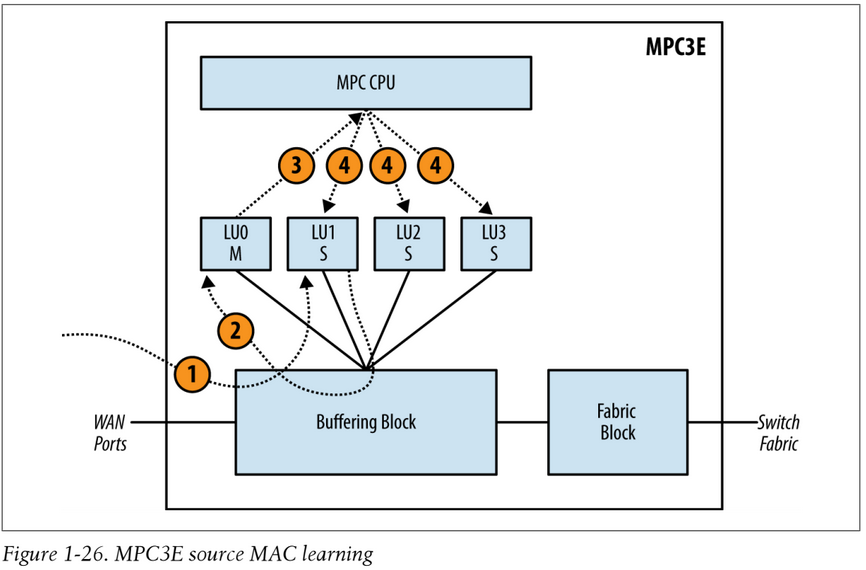
- A packet enters the Buffering Block and happens to be sprayed to LU1, which is designated as a Slave Lookup Block.
- LU1 updates its own table with the source MAC address. It then notifies the Master Lookup Block LU0. The update happens via the Buffering Block to reach LU0.
- The Master Lookup Block LU0 receives the source MAC address update and updates its local table accordingly. LU0 sends the source MAC address update to the MPC CPU.
- The MPC CPU receives the source MAC address update and in turn updates all Lookup Blocks in parallel.
Below are the steps for destination MAC learning from the fabric module (unlike the source MAC learning there's no concept of a master or slave Lookup Block, the Lookup Block that receives the packet from the switch fabric is responsible for updating the other Lookup Blocks.):
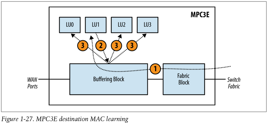
- A packet enters the Fabric Block and then Buffering Block. The packet happens to be sprayed to LU1. LU1 updates its local table.
- LU1 then sends updates to all other Lookup Blocks via the Buffering Block.
- The Buffering Block takes the update from LU1 and then updates the other Lookup Blocks in parallel. As each Lookup Block receives the update, the local table is updated accordingly.
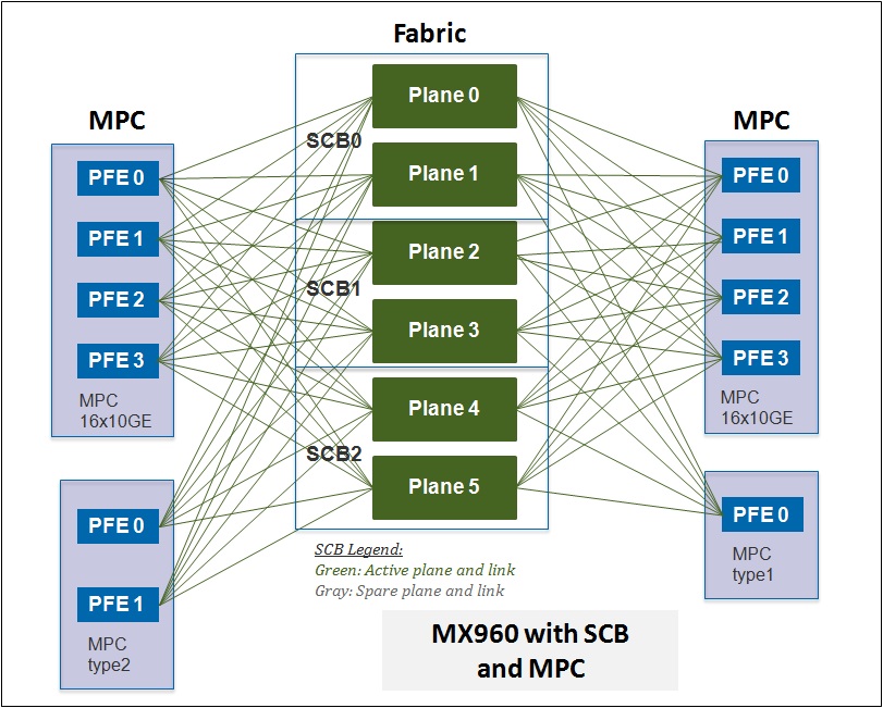
Switch Control Boards and Switch Fabric
The MX Series uses a distributed Packet Forwarding architecture. Each DPC/MPC contains either 1/2/4 PFEs, each of which is self-contained in terms of forwarding decisions. When the forwarding decision points to an output interface on a different PFE, which can either be on the same DPC/MPC or a different DPC/MPC, the packet needs to be sent across the Fabric Plane.
An SCB has three primary functions: switch data between the line cards, control the chassis, and house the routing engine. SBCs are the fabric forwarding modules within the MX series. The SCB is a single-slot card and has a carrier for the routing engine on the front. An MX480 can hold 2 SCBs (only one is required for forwarding, the second is a hot standby) and the MX960 can hold 3 (two are required for line rate forwarding, the third can be used for additional throughput or as a hot standby SCB).
The SCB or "SCB-MX" (not to be confused with SCBs from other Juniper product ranges) supports 120Gbps of full duplex throughput in the MX960 and 160Gbps in the MX240 and MX480, two SCBs are required in the MX240 and MX480 for line rate forwarding however in the MX960 even with 3 SCBs only MPC1 and MPC2 cards can achieve line rate forwarding (new FPCs require faster SCBs). The SCB is often used with the RE-1300 or RE-2000 and DPC line cards.
The SCBE or "SCBE-MX" supports 320Gbps of full duplex throughput in the MX240 and MX480 and 240Gbps in the MX960. The SCBE has a newer fabric ASIC called "XF" and is usually used with the RE-S-1800x4's and MPC line cards.
The SCBE2 or "SCBE2-MX" supports 340Gbps of full duplex throughput in an MX960 or 480Gbps on non-resilient throughput (MX240 and MX480). SCBE2s have an ever newer fabric ASIC called "XF2" and is usually used with the RE-S-1800x4's and MPC4 (or newer) cards.
An SCB can be redundant or not, which is how 3x SCBE2's in an MX960 for example can provide a bandwidth of up to 320Gbps per slot with redundant fabric support (2+1 SCBs) and 480Gbps per slot without redundant fabric support (3+0). SCB/SCBE example compatible line card: the MPC-3D-16XGE-SFPP line card has 120Gbps of throughput with an SCB (2+1 in MX960) and 160Gbps of throughput with an SCBE (3+1 in an MX960). An SCBE with the MPC-3D-16XGE-SFPP in an MX480 would provide the 160Gbps line rate to the MPC-3D-16XGE-SFPP card.
MPC4E and above line cards don't support the SCB-MX fabric cards.
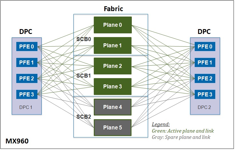
The switch fabric connects all of the ingress and egress PFEs within the chassis to create a full mesh. Each SCB has two switch fabrics (SF0 and SF1). Depending on the MX chassis each switch fabric can have either one or two fabric planes. The MX240 and MX480 support two SCBs for a total of four switch fabrics and eight fabric planes. The MX960 supports three SCBs for a total of six switch fabrics and six fabric planes.
When supporting 48 PFEs on the MX960, all of these connections on the switch fabric are completely consumed. On the MX480 each switch fabric only has to support 24 PFEs (half the number of line card slots), thus half of the connections aren't being used. On the MX240 and MX480 the unused connections are grouped together and another plane is created so that the unused connections can be used. The benefit is that the MX240 and MX480 only require a single SCB to provide line rate throughput, thus only require an additional SCB for 1 + 1 SCB redundancy.
The MX960 has to support twice the number of PFEs as the MX480, while maintaining the same line rate performance requirements. An additional SCB is mandatory to support these new scaling and performance requirements. The switch fabrics only support a single fabric plane because all available links are required to create a full mesh between all 48 PFEs. The MX960 supports up to three SCBs providing 2 + 1 SCB redundancy. At least two SCBs are required for basic line rate forwarding, and the third SCB provides redundancy in case of a SCB failure.
Regarding fabric CoS, Juniper supports two levels of priority: high and low. There are two queues per destination PFE: a high priority and a low priority queue. These two levels of priority are used when fabric congestion occurs. In this situation, scheduling occurs based on 95% for High Priority and 5% for Low Priority queue. Check fabric stats with "show class-of-service fabric statistics source 0 destination 11".
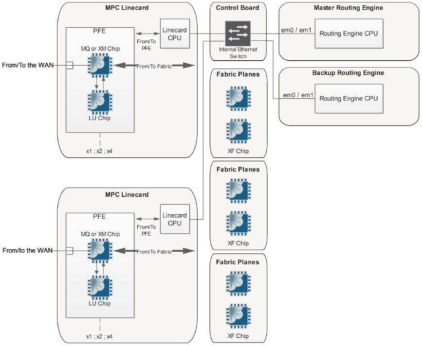
Line Card and RE CPU Paths
On a given MPC line card the line card CPU (running the μKernel) uses dual Ethernet connections to communicate with the routing engines and it uses a PCIe bus to program the ASICs (FIB updates to the LU chip or scheduling configuration to the MQ/XM chips). The PFE's ASICs communicate with each other and with the fabric chips via HSL2 (High Speed Link version 2) links.
The diagram below shows the RE packet flow path for "exception" packets or "punt" packets. Criteria for an exception packet are:
- Host inbound packets that are sent up to the control plane by the ingress PFE.
- Transit packets with an exceptional condition (TTL expired, IP Options, a reject action triggering ICMP destination unreachable) or a copy of a true transit packet (firewall log, RE-based sampling).
- Host-inbound control plane packets, like a ping to the host, ARP, LACP, routing packet sent to the local host or to a locally-bound 224.0.0.x multicast address.
- Host outbound packets: these packets are generated by the control plane and sent to the outside of the MX. They can be either crafted by the routing engine or by the linecard CPU. An example of the latter case is the generation of distributed keepalives (BFD, LACP) and specific ICMP unreachable packets.
Exceptions can be managed by the LU chip, the linecard's CPU (also known as the μKernel's CPU) or the routing engine's CPU. Some exception packets are actually discarded or fully processed by the linecard's ASIC, or by the μKernel's CPU, and hence are not punted to the final CPU at the routing engine. Some punt statistics can be seen with: "show pfe statistics exceptions fpc <fpc-slot>"
The diagrams below show how MPC cards can use all fabric plane links whereas DPC cards cannot:
Fabric Queueing, Grants and Mixing DCPE with MPC
Each PFE implements the fabric queuing and flow control mechanisms required to communicate to multiple other PFEs on the chassis at the same time. A request-grant mechanism (an arbiter) is used to implement flow control. Each PFE that wants to send a packet to a destination PFE sends a request, and only when the request is granted is it allowed to send the packet to the destination PFE.
When sending data packets across the chassis fabric if they are larger than 64 bytes they are split into 64 byte segments and then sent as a "J-Cell" from ingress PFE to egress PFE. The MX fabric uses "VoQ" Virtual output Queuing, similar to a Cisco ASR9000, where the ingress PFE must request from the Egress PFE a grant/approval before sending the J-Cell across the fabric to avoid congestion at the egress PFE (this helps with head of line blocking). Also the backplane has high and low priority fabric queues, traffic can be placed into the high priority fabric queue when setting the forwarding class for traffic.
An SCB with MPC2 card has twice the fabric capacity than needed available (SCB in MX480 can handle 160 Gbps of traffic and MPC2's have 2x ~40Gbps Trios), the additional capacity is used for binary multicast replication.
An SCB with the MPC-3D-16XGE-SFPP card uses all fabric capacity for unicast forwarding, multicast is replicated in a unary free manner.
If one mixes DCPE and MPC in FPCs in the same chassis in default configuration one cannot achieve linerate from the DPCE to Trio cards (with the MQ chip). This is because by default the MQ chip will use all fabrics, whereas DPCE won't. In an MX960 for example this means a DPCE is sending 40Gbps through two fabrics, but MQ expects to receive it's share 40Gbps through three fabrics. This means the MQ will only give grants to DPCE at 40/3*2 = 26Gbps. This can be addressed by changing the fabric mode from default performance to "redundant", causing MQ to use only two fabrics, allowing DPCE to send full 40Gbps to any given single MQ, with the down side that now all MPC1/2 Trio cards will still be able to achieve line rate (depending on the mixture of MPC and SCB cards).
MPC1 and MPC2 Ingress Packet Walkthrough
The only difference between the MPC1 and MPC2 at a high level is the number of Trio chipsets. Operationally they are equivalent. The following diagram shows the ingress packet flow direction:
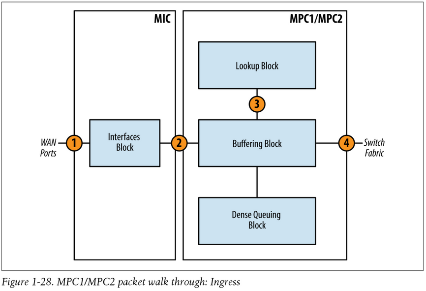
When an ingress packet is received from the WAN ports on the MIC and destined to another PFE:
- When a packet is received by the router, it is first handled by the MAC controller. This component provides an interface between the PHY layer and the MAC layer and delivers Ethernet Frames to the PFE. This is inside the Interfaces Block in the diagram, (IX chip on low end GE MICs) which will inspect each packet and perform pre-classification. Depending on the type of packet, it will be marked as high or low priority and passed to the Buffering Block.
- The packet enters the Buffering Block (QM chip or XM chip) and enqueue the packet as determined by the pre-classification and services the high priority queue first. These two chips have a pre-classifier engine, which is able to determine the packet type in a very simple manner (just like the IX chip on low end 1GE cards). Two classes are currently used and these two classes actually correspond to two WAN Internal Streams. A third stream is also available but not used. These streams are called Physical WAN Input Streams and have a meaning only within the PFE itself.
CTRL stream: (control stream, also known as medium stream) conveys protocol traffic (host-destined or in transit) as well as management traffic (for example, ping). At this level the line card can't figure out if the packet is for the host or for transit. This will be determined during the packet lookup, a task performed later by the LU chip.
BE stream: (Best Effort stream classified low) conveys all other types of traffic, not identified by the pre-classifier engine as control.
$ show precl-eng summary
$ show precl-eng 1 statistics
$ show mqchip 0 ifd
$ show xmchip 0 ifd list 0 # second 0 means Ingress – 1 Egress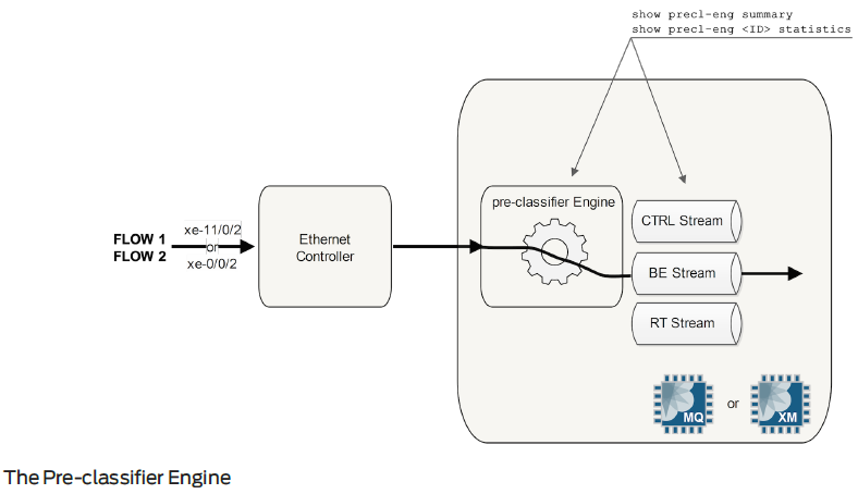
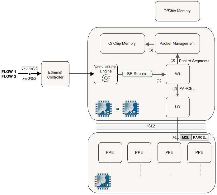
- After the pre-classification processing, the packet is handled by a new functional block of the MQ/XM chip: the WAN Input Block (WI). For each physical interface attached to the PFE, the WI Block receives packets from the three Physical WAN Input Streams (remember only two are used), after the pre-classification. This WI Block stores the packet for future processing in the packet buffer and generates a parcel by catching the first part of each packet.
Parcel: This is actually a chunk (also known as a first segment) of the real packet. This chunk contains all the packet headers and some other internal fields. The parcel has a variable length but also a maximum size of 320 bytes. Actually, if the packet size is less than 320 bytes the entire packet is taken into the parcel. Otherwise, if the packet size is above 320 bytes, only the first 256 bytes make it to the parcel.
Additional segments/chunks corresponding to the data that is not in the parcel are stored in the MQ/XM on-chip and off-chip memories.
J-Cells: When the entire packet needs to move from one PFE to another PFE through the fabric this packet is split in small cells that have a fixed size (64 bytes). - The packet enters the Lookup Block. A route lookup is performed and any services such as firewall filters, policing, statistics, and QoS classification are performed.
WI has generated the Parcel so the next step is packet lookup. The Parcel is sent to the LU (Lookup Unit) chip via the "LO" (LU Out) functional block of the MQ or XM Chip. The Parcel contains all the packet headers and no data which is enough information to perform route lookup, advanced packet handling, header modification, etc. There is no need to send the whole original packet to the LU chip.
The MQ or XM chip adds a header to the Parcel called the M2L header (MQ to LU). This header includes some information collected by the MQ or XM chip, like the Physical WAN Input Stream value. The other packet segments made by WI are pre-buffered in MQ/XM on-chip memory. The MQ/XM off-chip memory will be used later, during the queuing phase. The LU chip is split internally in several Packet Processor Engines (PPE). The traffic inside the LU chip is load balanced between all the PPEs. The LU can perform such tasks as packet lookup, traffic load balancing, uRPF check, packet classification, packet filtering, packet accounting, packet policing, and many others.
Note: In the case of cards like the MPC4E which has two LU chips per XM chip, the XM chip load balances parcels across the two (or more) LU chips. - Once The LU chip receives the parcel from the MQ or XM "LO" block, the LU chip first extracts the Physical WAN Input Stream ID from the M2L header. The field headers are parsed to see that EtherType is present (in the case of Ethernet at layer 2), if 0x800 is present for example the LU chip knows IPv4 is the payload of the Ethernet frame. An IPv4 sanity check is made which checks the packet total length and the checksum against the values carried in the IP header. If the sanity check fails, the packet is marked as "to be dropped" (drops will be performed by the MQ or XM chip).
The next step inside the LU chip is route lookup. There are several possible results for a transit packet: the forwarding next hop may be attached to the same PFE as the incoming interface (intra-PFE forwarding), or to a remote PFE (inter-PFE forwarding). When the LU chip computes the forwarding next hop, if there is equal-cost multipath (ECMP), or if the outgoing interface is a LAG (Link Aggregated Group), LU also performs the hash during route lookup. In this way, LU is responsible for load balancing traffic across ECMP or LAG's child links. To do this the LU chip extracts from the Parcel some fields of the packet: IP source/destination addresses, for example. Then it computes a hash key based on these fields. The hash is used to select the final and unique forwarding interface, among the several equal-cost choices, in the case of ECMP or LAG.
With the default static (non adaptive) load-balancing, some fields are mandatory and always used. For example, for IPv4 packets, IP source/destination addresses plus the IP protocol fields are included by default in the hash computation and cannot be removed. Other fields may be added or removed via configuration. One can use the following command to see the optional header fields being used in the hash calculation: request pfe execute target fpc0 command "show jnh lb". The "jsim" tool can be used inside the LU chip to build a Parcel by hand and simulate a route lookup and attain the output interface ID.
The ingress linecard is in charge of classifying the inbound packets and assigning them to the right forwarding class and drop/loss priority. The LU chip assigns these values but it does not perform any queuing or scheduling. These tasks are performed by the MQ/XM chip instead. LU chip of the ingress linecard not only assigns the packet to the right forwarding class/drop priority but also to the right fabric queue depending on the CoS configuration.
The LU job list in order is: packet analysis, route-lookup, load balancing, packet classification, and lastly fabric queue assignment. After all that the Parcel is sent back to the MQ/XM chip through the LU In Block (LI). The Parcel is "rewritten" before returning it to MQ/XM chip. LU adds additional information into a Parcel header. This may include:
- The first header called the L2M header is always present. The LU chip provides the MQ/XM chip with some information through this L2M header. The L2M header has a meaning only inside the PFE. It will be removed by the MQ/XM chip after processing. The L2M header conveys the queue assigned by the LU. This queue may be the fabric queue in the case of inter-PFE forwarding or the WAN Egress Forwarding Queue in case of intra-PFE Forwarding, or an egress lookup.
- The second header called the Fabric Header (FAB) has a meaning inside and outside the PFE. It allows inter-PFE forwarding. This header is added only when the packet should go to another PFE in order to reach its forwarding next hop. The Fabric Header conveys, along with other information, the next hop ID resulting from the packet lookup, the forwarding class, and the drop priority assigned by the ingress LU chip.
The diagram below shows the LU chip pipeline:
- Once the LU chip has done its job it returns the Parcel back to the MQ/XM chip, more specifically to the LI ("LU in") block of the MQ/XM chip.
The LI Block at MQ/XM moves the Parcel and the associated segments (previously stored at on-chip memory) to the off-chip memory. Only the pointer referring to the real packet is now stored at the MQ or XM on-chip memory. But keep in mind this pointer refers to the packet. Only pointers are queued. Real data stays in off-chip memory until it has to be forwarded towards either a remote PFE through the fabric (inter-PFE) or to a WAN interface (intra-PFE).
Now the MQ or XM chip knows that the packet should be forwarded to a remote PFE or local interface on the same PFE; If it is a remote PFE it also knows the destination PFE thanks to the fabric queue number carried in the L2M header. In the case of a packet being destined for a remote PFE it is enqueued into the switch fabric. If the packet is destined to a WAN port within itself, it will simply be enqueued back to the Interfaces Block.
When packets are queued and packet scheduling takes place, this job is performed by the SCHED block of the MQ or XM chip and it is in charge of providing CoS functions for packets in transit. Each PFE (MQ or XM chip) has two fabric queues (low and high) towards each possible remote PFE. Packet flows are queued into the correct fabric queue or fabric stream by the SCHED block of the MQ/XM chip, waiting for the approval of the remote PFE before sending them through the fabric. The new functional block FO (Fabric Out) part of MQ/XM chip sends the entire packet (actually the Parcel with its FAB header generated by LU chip, plus the other packet segments) to the right destination. - In the case of Inter-PFE traffic, packets are sent across the fabric in J-cells (64 byte cells). The MX fabric is made up of several fabric planes. The cells of a given packet are load-balanced over these several planes in a round-robin manner. A sequence number is assigned to each cell, to ensure cell re-ordering on the egress PFE side.
The group of cells (of a given packet) does not go directly from a source PFE to a destination PFE. For every single cell, the source PFE needs to first send a request through a specific fabric plane to the remote (destination) PFE. In return, the destination PFE acknowledges the request by sending back a reply over the same fabric plane. When the reply is received by the source PFE, the data cell can be sent over the fabric. The request / grant cells implement a flow control mechanism, but they carry no traffic data themselves. Actually, request/grant cells are piggy-backed with other data cells but they are logically independent. This mechanism also prevents PFE oversubscription. If the destination PFE is congested, it silently discards incoming requests. This indirectly puts pressure on the source PFE, which does not see incoming grants and as a result buffers the packet chunks for some time. The outcome may be RED or TAIL drops.
The diagram below shows the Ingress PFE process end-to-end (click for larger image):
MPC1 and MPC2 Egress Packet Walkthrough
Egress packets are handled a bit differently. The major difference is that the Dense Queuing Block will perform class of service, if configured, on egress packets.
- The FI block (Fabric Input) of the egress PFE receives the cells coming from the different fabric planes. FI is in charge of re-ordering the cells of a given packet before the packet is sent to off-chip memory. Only the Parcel, with its FAB header is sent to the egress LU chip. The packet enters the Buffering Block. If class of service is configured, the Buffering Block will send the packet to the Dense Queuing Block.
- The packet enters the Dense Queuing Block. The packet will then be subject to scheduling, shaping, and any other hierarchical class of service as required. Packets will be enqueued as determined by the class of service configuration. The Dense Queuing Block will then de-queue packets that are ready for transmission and send them to the Buffering Block.
- The Buffering Block receives the packet and sends it to the Lookup Block. A route lookup is performed as well as any services such as firewall filters, policing, statistics, and accounting. The Parcel and its FAB header are sent to the LU chip of the egress PFE. The MQ/XM chip adds the M2L header. For "egress" lookup the M2L conveys the Input fabric queue number.
The egress LU chip performs several tasks. It first extracts information from the M2L and FAB headers. Based on the NH ID (Next Hop ID) and some Parcel fields (like next hop's IP for ARP resolution) it can deduce the forwarding next hop and build the Layer 2 header. This includes pushing or popping headers like MPLS, VLAN, etc., if needed. Moreover, based on the CoS information (forwarding class and loss priority) it can assign the right WAN Physical Output Queue to use and also perform CoS packet re-writing. Once the packet (actually the Parcel) has been re-written, it goes back to the MQ/XM Chip. The FAB Header has been removed and only the L2M header is now present. This header conveys the WAN Output Queue number.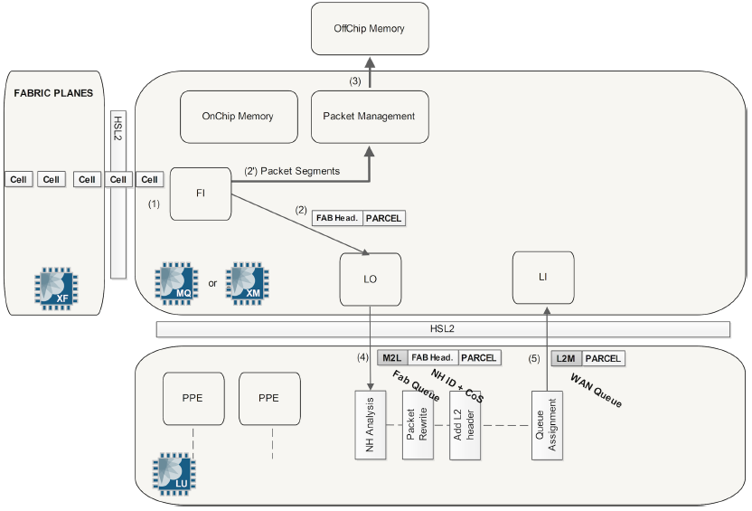
- The parcel moves back to the MQ/XM chip via the LI block (without the FAB header), then the L2M header is decoded and removed. The MQ/XM knows on which WAN queue of the SCHED block the packet has to be queued. As mentioned previously, the real packet stays in memory and the only information queued is data pointers. Therefore, the MQ/XM pushes the Parcel to off-chip memory, where the remaining packet segments are already. When the scheduler for the output physical interface decides that the packet can be forwarded (or the pointer is de-queued), it sends a notification to the last functional block WO (WAN Output). This block retrieves packet segments from the off-chip memory, reassembles the packet, and forwards it to the MAC controller to finally leave the router.
For MQ/XM-based queueing (e.g. queuing management not delegated to QX or XQ chip) the default maximum data buffer value is 100ms. However, the temporal buffer is higher (in ms) with per-unit-scheduler at low shaping rates.
The diagram below shows the egress PFE process end-to-end (click for larger image):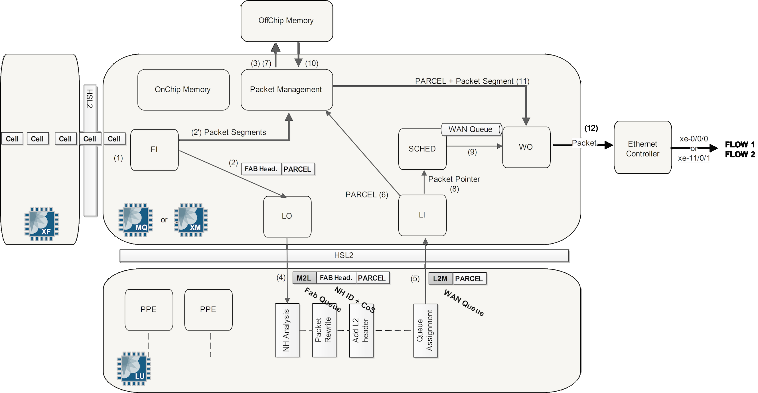
MPC3 Ingress Packet Walkthrough
The packet flow of the MPC3E is similar to the MPC1 and MPC2, with a couple of notable differences being the introduction of the Fabric Block and multiple Lookup Blocks. The diagram below shows the packet ingress flow path:
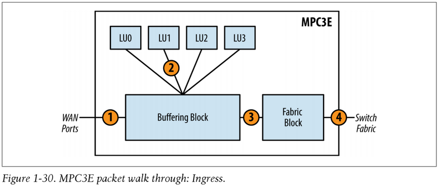
- The packet enters the Buffering Block from the WAN ports and is subject to pre-classification. Depending on the type of packet, it will be marked as high or low priority. The Buffering Block will enqueue the packet as determined by the pre-classification and service the high-priority queue first. A Lookup Block is selected via round-robin and the packet is sent to that particular Lookup Block.
- The packet enters the Lookup Block. A route lookup is performed and any services such as firewall filters, policing, statistics, and QoS classification are performed. The Lookup Block sends the packet back to the Buffering Block.
- The packet is sent back to the Fabric Block and is enqueued into the switch fabric where it will be destined to another PFE. If the packet is destined to a WAN port within itself, it will simply be enqueued back to the Interfaces Block.
- The packet is sent to the switch fabric.
MPC3 Egress Packet Walkthrough
Egress packets are very similar to ingress, but the direction is simply reversed. The only major difference is that the Buffering Block will perform basic class of service, as it doesn't support enhanced queuing due to the lack of a Dense Queuing Block. The diagram below shows the egress packet flow in MPC3E:
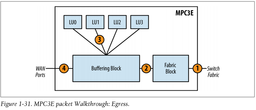
- 1. The packet is received from the switch fabric and sent to the Fabric Block. The Fabric Block sends the packet to the Buffering Block.
- The packet enters the Buffering Block. The packet will then be subject to scheduling, shaping, and any other class of service as required. Packets will be enqueued as determined by the class of service configuration. The Buffering Block will then de-queue packets that are ready for transmission and send them to a Lookup Block selected via round-robin.
- The packet enters the Lookup Block. A route lookup is performed as well as any services such as firewall filters, policing, statistics, and QoS classification. The Lookup Block sends the packet back to the Buffering Block.
- The Buffering Block receives the packet and sends it to the WAN ports for transmission.
A high-level view of the life of a packet inside Trio 6:
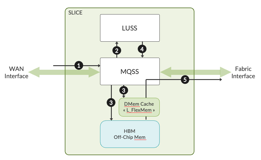
- A packet is received on the MQSS block either from the WAN or Fabric interface.
- Pre-classification decides the priority of the packet to make sure that high priority control traffic is protected even if the PFE is oversubscribed.
- If the incoming packet size is <=224 bytes, the complete packet will be sent to the LUSS. If the incoming packet is > 224 bytes, the packet is split into HEAD (192 bytes) and TAIL. A reorder context and a reorder ID is created. Then, HEAD is sent to LUSS for processing.
- The tail of the packet is either sent to on-chip SRAM (M_FlexMem) or off-chip HBM.
- The incoming packet gets processed in the PPEs in LUSS. Once LUSS has finished processing, the modified packet or HEAD is sent back to MQSS. Here reorder entry of the packet is validated and, once it becomes eligible, it is sent to the scheduler.
- Once the packet becomes eligible to be sent out of PFE, the content will be read from M_FlexMem or HBM and the packet will be sent out via the WAN/Fabric interface.
Time for a lie down.
Previous page: JunOS - Committing and Rolling-back
Next page: MX Series LU-chip Overview