Date created: Friday, October 6, 2017 2:43:36 PM. Last modified: Tuesday, December 26, 2023 11:38:16 AM
MX Series LU-chip Overview
References:
Juniper MX Series - https://www.safaribooksonline.com/library/view/juniper-mx-series/9781491932711/ch01.html
Juniper MX Series (2nd Edition) - http://shop.oreilly.com/product/0636920042709.do
https://www.juniper.net/documentation/en_US/junos/topics/reference/command-summary/show-chassis-fpc.html
https://www.juniper.net/documentation/en_US/junos/topics/concept/resource-monitoring-usage-calculation.html
https://www.juniper.net/documentation/en_US/junos/topics/concept/resource-monitoring-overview.html
https://community.juniper.net/blogs/deepaktr/2022/06/29/mx10000-lc9600-deepdive
Contents:
Trio Chipset / PFE Recap
Linecard Recap and Lab Topology
The LookUp Block and Forwarding
PFE/LU Memory
PFE/LU FIB Scaling
FPC/PFE Memory Monitoring
Trio Chipset / PFE Recap
PFEs are made of several ASICs, which may be grouped into four categories:
- Routing ASICs: LU or XL Chips. LU stands for Lookup Unit and XL is a more powerful (X) version. The LU chip performs packet lookup, packet firewalling and policing, packet classification, queue assignment, and packet modification (for example, push/swap/push MPLS headers, CoS remarks, etc.). This chip relies on combined on-chip/off-chip memory integration. The FIB is stored in off-chip memory.
- Forwarding ASICs: MQ or XM Chips. MQ stands for Memory and Buffering/Queuing, and XM is a more powerful (X) version. The MQ chip is in charge of packet memory management, queuing packets, "cellification" and interfacing with the fabric planes. It features both fast on-chip (SRAM) memory and off-chip memory. The XM chip introduces the concept of WAN Groups which can be considered as a virtual PFE. In case of the MPC3E, WAN Group 0 manages the MIC 0 and WAN Group 1 manages the MIC 1. The MPC3E's XM chip doesn't directly connect to the fabric planes, one XF ASIC, programmed in Fabric Offload mode plays the role of gateway between the PFE and the fabric.
- Enhanced Class of Service (CoS) ASICs: QX or XQ Chips. QX stands for Dense Queuing and again, XQ is a more powerful (X) version. These chips provide advanced QoS/CoS features like hierarchical per-VLAN queuing.
- Interface Adaptation ASICs: IX (interface management for oversubscribed MICs) and XF (only on MPC3E).
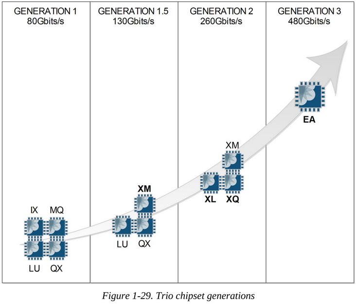
Caveat Emptor: Even Juniper's own documentation mixes up the naming for the different generations of Trio, so it is also a bit mixed here below too!
The first generation Trio PFE contained the LU and MQ chips and optionally the QX chip if enhanced QoS was required, and optionally the IX chip if oversubscription management was required. This generation includes MPC types 1 and 2, as well as the MPC 16x10GE. Gen 1 Trio's support up to 40Gbps full-duplex (actually slightly less as this is the throughput with the most optimal lab conditions!). MPC1 cards have a single Gen 1 Trio an MPC2 cards have two Gen 2 Trios.
The next generation of Trio PFEs is sometimes called generation 1.5 or the Enhanced PFE, which updated the MQ buffering chip to XM which supports speeds up to 130Gbps full-duplex (ideal lab conditions only!) to support 40Gbps and 100Gbps interfaces. To support this a faster XM chip and multiple LU chips were used in the PFE for the first time. This is the PFE used on MPC3E and MPC4E cards. MPC3E cards use one Gen 1.5 Trio and MPC4Es use two Gen 1.5 Trios. Some people consider this the second generation.
The actual second generation of Trio PFEs enhanced the Lookup and Dense Queuing Blocks: the LU chip became the XL chip and the QX chip became the XQ, respectively. This PFE also uses the XM chip. This second generation of Trio equips the MPC5E, MPC6E and the NG-MPC2E and NG-MPC3E line cards. This PFE support 130Gbps full-duplex (ideal lab conditions only!). MPC5E cards use a single Gen 2 Trio and MPC6E cards use two Gen 2 Trios. Some people consider this the third generation.
The third generation of Trio embeds all the functional blocks in one ASIC (XL, XM and XQ). Called the "Eagle" ASIC, also known as the EA chipset, this Gen 3 Trio supports 480Gbps full-duplex and powers the newer MPC7E, MPC8E, and MPC9E cards. MPC7Es and MPC8Es use Gen 3 Trios limited to 240Gbps each. MPC9Es use Gen 3 Trios that are unlimited. Some people consider this the fourth generation.
The fourth generation of Trio is the ZT chipset, also known as "Penta", which powers the MPC10, 11 and 12 cards. These are rated for 500Gbps full-duplex and multiple are packaged together to support 1.5Tbps (full duplex) in MPC10 cards and 4.0Tbps in MPC11 and MPC12 cards (full/half duplex?). Some people consider this the fifth generation.
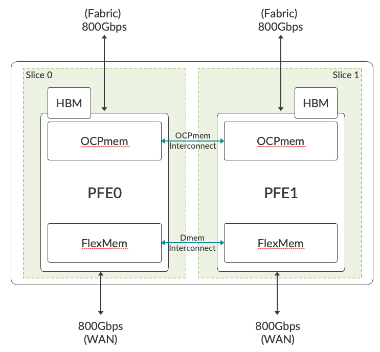
The "sixth"? generation of Trio is a seven-nanometre (7nm) ASIC with a core clock frequency of 1.2GHz, which provides 1.6Tbps of full-duplex forwarding capacity (36x 56Gbps SerDes towards the fabric and 32 towards the front ports). Trio 6 is made of two slices, each having its own Packet Forwarding Engine (PFE) providing 800Gbps of full-duplex throughput. The two slices on Trio 6 have a combination of on-chip and off-chip memories. It uses internal SRAM as on-chip memory (OCPMEM) to implement caches for high bandwidth and low latency accesses to lookup data structures. This helps in reducing the power budget required for frequent read-write operations needed for packet processing. HBM is used as off-chip memory for delay bandwidth buffer, and high scale flow table (Jflow) storage. On-chip (FlexMem) and off-chip (HBM) memories are shared between the two slices. Sharing of processing memory allows a single copy of the Forwarding Information Base (FIB). This architecture offers better resource utilization when both the slices are not using memory equally.
The numbers on the picture below aren't accurate*
Gen 6 Trio Overview
Linecard Recap and Lab Topology
In the output below it can be seen that an MX-MPC2E-3D-Q Modular Port Concentrator is present, which has two PFEs (one per MIC slot), MIC0 contains Modular Interface Card MIC-3D-4XGE-XFP and MIC1 contains MIC-3D-2XGE-XFP. Note that due to the MPC being a –Q model the output below also shows two QX chips at the end, one for each PFE:
> show chassis hardware
Item             Version  Part number  Serial number     Description
…
FPC 0            REV 09   750-038493   12345678          MPCE Type 2 3D Q
  CPU            REV 04   711-038484   12345678          MPCE PMB 2G
  MIC 0          REV 30   750-028387   12345678          3D 4x 10GE  XFP
    PIC 0                 BUILTIN      BUILTIN           2x 10GE  XFP
      Xcvr 0     REV 01   740-011607   123456789012      XFP-10G-LR
      Xcvr 1     REV 01   740-031833   123456789012      XFP-10G-LR
    PIC 1                 BUILTIN      BUILTIN           2x 10GE  XFP
      Xcvr 0     REV 01   740-031833   123456789012      XFP-10G-LR
      Xcvr 1     REV 01   740-031833   1234567           XFP-10G-LR
  MIC 1          REV 21   750-028380   1234567           3D 2x 10GE XFP
    PIC 2                 BUILTIN      BUILTIN           1x 10GE XFP
      Xcvr 0     REV 01   740-031833   1234567           XFP-10G-LR
    PIC 3                 BUILTIN      BUILTIN           1x 10GE XFP
      Xcvr 0     REV 01   740-031833   123456789012      XFP-10G-LR
  QXM 0          REV 06   711-028408   12345678          MPC QXM
  QXM 1          REV 06   711-028408   12345678          MPC QXM
In the output below it can be seen that each PFE inside the MPC2E-3D-Q card has an LU chip and an MQ chip and also a QX chip (note the -Q in the card name for "enhanced queueing). Note there is one IX chip present also, this is on the MIC-3D-2XGE-XFP card.
> request pfe execute command "show jspec client" target fpc0
SENT: Ukern command: show jspec client
GOT:  ID       Name
GOT:   1       LUCHIP[0]
GOT:   2       QXCHIP[0]
GOT:   3       MQCHIP[0]
GOT:   4       LUCHIP[1]
GOT:   5       QXCHIP[1]
GOT:   6       MQCHIP[1]
GOT:   7       IXCHIP[2]
This lab box actually has 2x MPC2E cards and 1x DPC card installed (slots 0 and 1 are MPC2E FPCs and slot 2 is the DPC FPC). Below it can be seen that the MPC2E card in slot 0 has an MQ chip for advanced classification used in the pre-classification engine:
me@lab-mx> request pfe execute target fpc0 command "show precl-eng summary"
SENT: Ukern command: show precl-eng summary
GOT:
GOT:  ID  precl_eng name       FPC PIC   (ptr)
GOT: --- -------------------- ---- ---  --------
GOT:   1 MQ_engine.0.0.16       0   0  4e4e2fd0
GOT:   2 IX_engine.0.1.22       0   1  4e7c9b60
LOCAL: End of file
The non-Q model MPC2E has no MQ chip as shown below:
me@lab-mx> request pfe execute target fpc1 command "show precl-eng summary"
SENT: Ukern command: show precl-eng summary
GOT:
GOT:  ID  precl_eng name       FPC PIC   (ptr)
GOT: --- -------------------- ---- ---  --------
GOT:   1 IX_engine.1.0.20       1   0  4e4bb9e0
LOCAL: End of file
Here one can see that each FPC has two PFEs (these are two Gen 1. Trio PFEs for the first two FPCs as they are MPC2E and two I-chip PFEs on the DPC card):
me@lab-mx> show chassis fabric fpcs | match "FPC|PFE"
Fabric management FPC state:
FPC 0
  PFE #0
  PFE #1
FPC 1
  PFE #0
  PFE #1
FPC 2
  PFE #0
  PFE #2
The MPC2E cards have twice as much CPU DRAM compared to the DPC card:
me@lab-mx> start shell pfe network fpc0
NPC platform (1067Mhz MPC 8548 processor, 2048MB memory, 512KB flash)
NPC0(lab-mx vty)# exit
me@lab-mx>
me@lab-mx> start shell pfe network fpc2
ADPC platform (1200Mhz MPC 8548 processor, 1024MB memory, 512KB flash)
ADPC2(lab-mx vty)# exit

me@lab-mx> show chassis fpc
                     Temp  CPU Utilization (%)   Memory    Utilization (%)
Slot State            (C)  Total  Interrupt      DRAM (MB) Heap     Buffer
  0  Online            36     10          0       2048       18         14
  1  Online            33      7          0       2048       18         14
  2  Online            27      5          0       1024       23         20
  3  Empty
  4  Empty
  5  Empty
The LookUp Block and Forwarding
The Lookup Block is part of the LU, XL, and EA ASICs. The Lookup Block has multi-core processors to support parallel tasks using multiple threads, these are the Packet Processing Engines (PPEs). MX PPEs are Run-To-Completion packet forwarding engines, as opposed to fixed pipeline stages. The PPEs run independently of each other. Each PPE can run for a varying amount of time depending on the complexity of the code that is needed to run, in order to process a packet. This means that packet recirculation is not required like it is in a fixed pipeline, when implementing more advanced features, but it does mean that latency is variable which is not the case in a fixed pipeline.
As packets are received by the Buffering Block, the packet headers are sent to the Lookup Block for additional processing (the tail/payload is sent into packet memory, which could be on or off chip). This chunk of packet is called the Parcel (up to 256 bytes of headers are packed into the Parcel). The LU dipatcher sends the parcel to the next free PPE for processing. All processing is completed in one pass through the Lookup Block regardless of the complexity of the workflow (RTC). Once the Lookup Block has finished processing, it sends the modified packet headers back to the Buffering Block to send the packet to its final destination.
Side Note on Hypermode:
Starting with Junos 13.x, Juniper introduced a concept called Hypermode. The lookup chipset (LU/XL chips) are loaded with a "full" micro-code by Junos which supports all the functions from the more basic to the more complex (BNG for example). Each function is viewed as a functional block and depending on the configured features, some of these blocks are used during packet processing. Even if all blocks are not used at a given time, there are some dependencies between each of them. These dependencies request more CPU instructions and thus more time, even if the packet just simply needs to be forwarded. To improve the performance at line rate for small packet sizes, the concept of Hypermode was developed. It disables and doesn't load some of the functional blocks into the micro-code of the lookup engine, reducing the number of micro-code instructions that need to be executed per packet.
The Gen 1 Trio has one LU chip per PFE and each LU chip has 16 PPEs. Within an LU chip incoming requests are sprayed across all 16 PPEs in a round-robin fashion to spread the load and each PPE has 20 contexts so that a PPE can work even when one thread is stalled (I/O wait for example). The LU chip does not perform work in constant-time (FIFO is not guaranteed for the LU complex, only for a given PPE).
The Gen "1.5" or Enhanced Trio on the MPC3E and MPC4E cards have the XM chip so two LU chips are used per XM chip (two LU chips per PFE, meaning 32 PPEs per PFE). The XM chip load balances parcels across the two LU chips (which load-balance over their respective 16 PPEs).
Gen 3 Trios have 64 PPEs.
Gen 4 Trios have 96 PPEs.
Gen 5 Trios also have 96 PPEs.
Gen 6 Trios have 160 PPEs (80 per slice?).
The diagram below shows the components of one of the two slices inside a Gen 6 Trio:
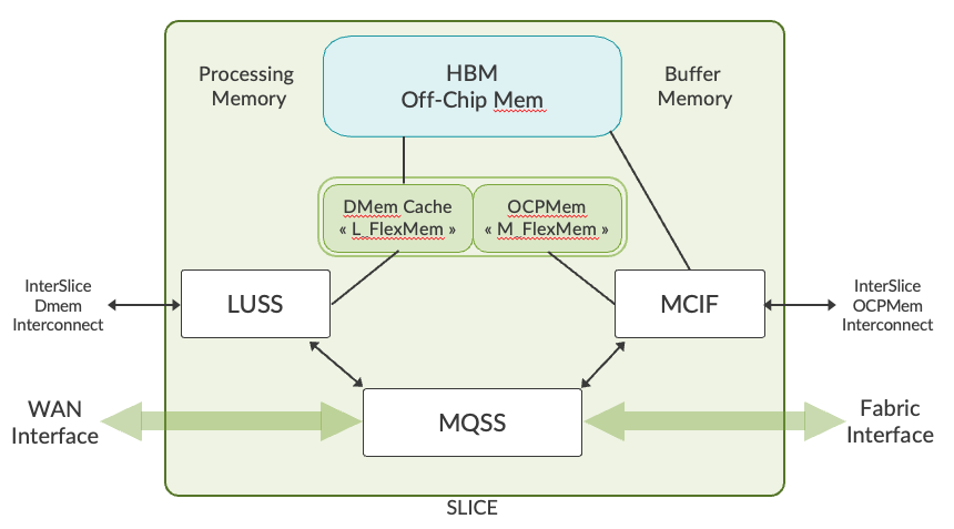
Internally each slice is built on the following main components:
- LUSS (Lookup Sub-system) provides all packet processing functions such as route/label lookup, firewall, and multi-field packet classification. This sub-system holds an array of PPEs to perform these functions.
- MQSS (Memory and Queuing Sub-system) provides data paths and rich queuing functionality. It acts as an interface between WAN and Fabric. It has a pre-classifier where packets are categorized as low/high priority. Unlike initial generations of Trio where an Extended Queuing Sub-System (XQSS) was used to provide queuing functionality, MQSS on Trio 6 integrates this function. It reduces the footprint utilization in the PCB (Printed Circuit Board) and improves the power performance without any compromise on functionality.
- MCIF (Memory Control Interface) is the interface to HBM and on-chip FlexMem.
- L_FlexMem (LUSS FlexMem) is a large cache for processing memory.
- M_FlexMem (MQSS FlexMem) is an on-chip packet buffer.
PFE/LU Memory (Trio Gen 1-3)
The LU chip has external memory consisting of RLDRAM and DDR3 SDRAM. From a logical perspective, the LU has two categories of memory, Data Memory (DMEM) and Optional Memory (OMEM). The DMEM is physically accessible by all functional blocks within the LU. The use of OMEM is limited to the sFlow application, for inline flow export capabilities. The DMEM is further separated into a small on-chip SRAM called Internal DMEM (IDMEM) and a large off-chip RLDRAM called External DMEM (EDMEM). The IDMEM is used for small fast data elements and the EDMEM is used for the remainder. OMEM is configured to reside on DDR3 SDRAM. In the current designs IDMEM includes ~3 MB of memory arranged in 4 banks. EDMEM consists of four 64 MB devices, with either 2-way or 4-way replicated data elements.
IDMEM (Internal Data Memory) is stored in on-chip SRAM [to the Lu-chip] and contains forwarding data structures such as the routes (I think it stores the compressed JTREE?). IDMEM is a portion of the total DMEM.
The EDMEM (External Data Memory) is 4 channels of RLDRAM 36-bits wide. EDMEM stores the remaining data structures that cannot be stored in IDMEM such as firewall filters, counters, next hops FIB entries, Layer 2 rewrite data, encapsulations, and hash data. These memory allocations aren't static and are allocated as needed. There is a large pool of memory and each EDMEM attribute can grow dynamically. EDMEM also forms a portion of the total DMEM.
OMEM (Optional Memory) is off-chip DDR3 DRAM and is used in conjunction with the Hash/Flowtable/Per-flow statistics/Mobilenext block. 2 channels that are 16-bits wide are used to store this. E series MPC cards have twice the DDR3 RAM than the non-E variants.
Along with a policer or counter block, there is also the Internal Memory Controller (IMC) that is responsible for implementing and managing the IDMEM or the on-chip portion of the LU memory.
For external memory controlling, External and RLDRAM Memory Controller (EMC) is responsible for implementing and managing the EDMEM or the off-chip RLDRAM portion of the LU memory. The LU differs from previous ASICs in that the functional blocks within the LU do not have 'private' memories associated with each functional block, rather the LU has a large memory that is shared by all of the blocks. Different memory regions in the external RLDRAM are replicated 1-way, 2-way and 4-way. Applications pick the memory based on their needs. Data-structures with high write rate (e.g. policers) would be allocated in pages with no replication, data-structures that are mostly static and seldom used are allocated in pages with 2-way replication, and data-structures that are mostly static and used more often are allocated in pages with 4-way replication. The counter block in LU supports replicated memory. READ/WRITE accesses to counters are balanced across the copies currently in use.
The command output below shows some of the memory types for LU chip 0 which is in PFE0 as this MPC2E only has 2 PFEs, LU chip 1 is in PFE1. This means there is 576MBs of RLDRAM per PFE as there is one LUchip per PFE in MPC2E cards:
NPC0(lab-mx vty)# show luchip 0
...
    RLDRAM:  576 Mb by 4 devices at 533 MHz.
      DDR3:  2048 Mb by 2 devices at 733MHz/CL10.
      TCAM:  Installed.
The MPC2E card also has 734MBs of RLDRAM that is used by the FPC CPU (not shown here). The output below shows the usage of each memory pool in PFE 0 in MPC 0:
> start shell pfe network fpc0
NPC0(lab-mx vty)# show jnh 0 pool summary
                Name        Size      Allocated     % Utilization
               EDMEM    33554368       16724615               49%
               IDMEM      315392         301773               95%
                OMEM    67108864       33202208               49%
         Shared LMEM    67109888      100311171               21%
DMEM is physically accessible by all blocks within the LU. DMEM is separated into: small on-chip (384K DWords) Internal DMEM (IDMEM) and large off-chip RLDRAM (32M DWords) External DMEM (EDMEM). The IDMEM is used for small and fast data elements and the EDMEM is used for the remainder.
SRAM IDMEM for LUchip is ~3MBs arranged 4 banks. It can hold 384K DWords: 384,000 * 8 = 3.072MBs. IDMEM is used by PPEs for a parity check during read/write operations.
RLDRAM EDMEM for LUchip is 4 channels, each 36-bits wide, each 256MBs (288MBs with parity) in size. The extra bit per byte is used to support ECC. Using 64-bit Double Words (which would be stored as 9 bytes with parity) means that 32 MDW (Mega Double Words) can be stored in 288MBs of RLDRAM (72MBs of each RLDRAM channel is combined to make 288MBs, the data is 4-way replicated). 288MBs / 9 bytes (8 bytes + 1 bit parity per byte) == 32MDW. Accessed EDMEM will be replicated 4 times for improving performance of WRITE-FEW-READ-OFTEN data elements. Apparently anything from the MX80 to the T4k FPC5 all have same 256MB (288MBs with parity) RLDRAM for LU. EDMEM stores next-hop and firewall filter entries, accessed by PPEs.
DDR3 OMEM is 2 channels, each 16-bits wide. OMEM is used for Hashing, Mobilenext, Flowtable, Per-flow statistics etc.
TCAM isn't used in the Trio chipset.
LMEM is an internal memory in LU/XL ASIC chip. It has private and shared regions for Packet Processing Engines.
External Transaction (XTXN) are used to move data from PPE to different blocks within LU.
For statistics on individual PPEs use the command:
$ request pfe execute target fpc0 command "show luchip X ppe X"
The following command shows the DMEM usage by application (e.g. Firewall, Next-hop, Encapsulations):
NPC0(lab-mx vty)# show jnh 0 pool bytes
                Name     MemType            Total(b)      Used(b)    (%)    Free(b)    (%)

            Next Hop     EDMEM              33553920      25018080   74%    8535840    26%
                         IDMEM              2457600       2402216    97%    55384      3%

            Firewall     EDMEM              16777216      342456     2%     16434760   98%

            Counters     EDMEM              50331648      18449328   36%    31882320   64%
                         IDMEM              131072        28064      21%    103008     79%

                LMEM     LMEM               8192          792        9%     7400       91%

                HASH     EDMEM              133693440     191066112  >99%   4237594624 < 1%

              ENCAPS     EDMEM              111448064     191066112  >99%   4215349248 < 1%

          UEID_SPACE     0x01c00000         1048576       131        < 1%   1048445    >99%

   UEID_SHARED_SPACE     0x01bf0000         65536         4          < 1%   65532      >99%
More detailed stats per application pool can be seen with "show jnh 0 pool stats <number>" (0-NH, 1-DFW, 2-CNT, 7-UEID, 8-SHARED_UEID).
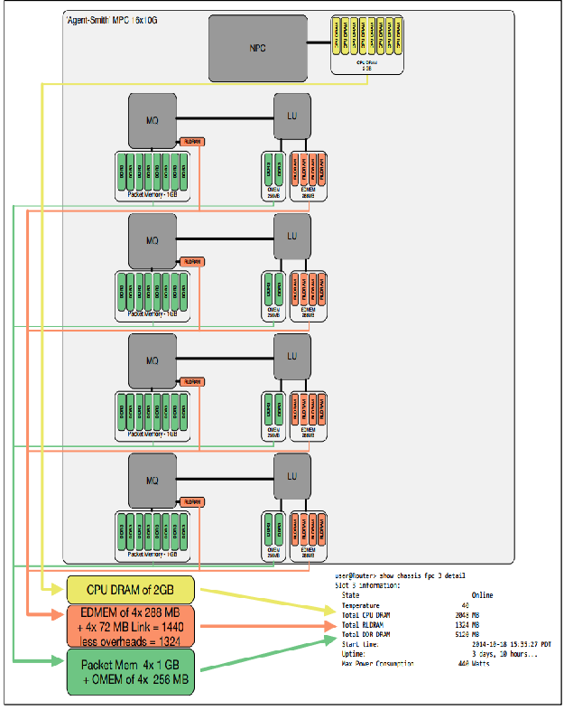
Below is a frustratingly low resolution image of MPC card memory blocks:
PFE/LU FIB Scaling
In the below output from an example MX480 one can see the EDMEM usage for PFE0 in FPC0 (an MPC2E with two PFEs)
# request pfe execute target fpc0 command "show jnh 0 pool usage"
# or "start shell pfe network fpc0" then "show jnh 0 pool usage"
NPC0(lab-mx vty)# show jnh 0 pool usage
EDMEM overall usage:
[NH///////|FW////////|CNTR///////////|HASH////////////|ENCAPS////|------------------]
0        4.0        8.0            14.0             20.7       24.8               32.0M

Next Hop
[****************************|------------------] 4.0M (61% | 39%)

Firewall
[|----------------------|RRRRRRRRRRRRRRRRRRRRRRRR] 4.0M (<1% | >99%)

Counters
[*************************|---------------------------------------------] 6.0M (35% | 65%)

HASH
[********************************************************************************] 6.7M (100% | 0%)

ENCAPS
[************************************************] 4.1M (100% | 0%)

Shared Memory - NH/FW/CNTR/HASH/ENCAPS
[--------------------------------------------------------------------------------] 7.2M (0% | 100%)
While portions of this memory are reserved for each function, the memory system is flexible and allows areas with heavy use to expand into unused memory. As a result it's not uncommon to check resource usage and find it seems alarmingly high, e.g. 98% utilised, only to find one can keep pushing that scale dimension and later find the pool has been dynamically resized.
The command output above is based on the allocation of Mega Double Words (MDW, where "Mega" here is 10^6 like the SI prefix meaning "million" in English), with each Word being 32 bits (4 bytes) in length thus a Double Word is 64 bits (8 bytes) in length.
It can be seen that 4M are allocated for next hop info and 6M allocated for counters etc. In this display, 1M equates to 1 MDW or 1M * 8B (1 million * 8 Double Words), which equals 8MBs. The first Trio PFE (MPC1/MPC2 cards) can allocate up to 88 MB per PFE to hold filter and policer structures. NH is limited to a maximum of 11 MDWs. What matters for capacity planning is overall utilization and how close NH is to having 11MDW, and if so, how much of that is used. To survive negative events Juniper suggests that no more than 80-85% of the maximum 11 MDWs be used.
In the below example output NH usage has grown from the default allocation of 4 MDWs to 8MDWs and 84% of those 8MDWs are used:
NPC7(gallon vty)# sho jnh 0 poo usage
EDMEM overall usage:
[NH//////////////////|FW////////|CNTR///////////|HASH////////////|ENCAPS////|--------]
0                   8.0       12.0            18.0             24.7       28.8     32.0M

Next Hop
[*******************************************************************|------------] 8.0M (84% | 16%)

Firewall
[*|------------------|RRRRRRRRRRRRRRRRRRRR] 4.0M (3% | 97%)

Counters
[***********************|------------------------------------] 6.0M (38% | 62%)

HASH
[*******************************************************************] 6.7M (100% | 0%)

ENCAPS
[****************************************] 4.1M (100% | 0%)

Shared Memory - NH/FW/CNTR/HASH/ENCAPS
[**************************************|------------------------------------------] 7.2M (48% | 52%)
There are no fixed scaling numbers for Trio PFEs. IPv4 and IPv6 routes shared the same memory space and each IPv6 route uses double the amount of memory that an IPv4 route requires so each IPv6 route means two less IPv4 routes can be stored.
PFE route table size can be checked with the following command:
$ request pfe execute target fpc0 command “show route summary”
NPC0(lab-mx vty)# show route summary

IPv4 Route Tables:
Index         Routes     Size(b)
--------  ----------  ----------
Default       646515    82753916
1                 23        2940
2                  6         764
4                  5         636
5               3757      480892
7                 82       10492
8                 42        5372
9                 22        2812
10                60        7676
11                15        1916
12              2058      263420

MPLS Route Tables:
Index         Routes     Size(b)
--------  ----------  ----------
Default          778       99580
6                  1         124

IPv6 Route Tables:
Index         Routes     Size(b)
--------  ----------  ----------
Default            4         532
1                  7         952
4                  4         532
5                  4         532
7                  4         532
8                  4         532
9                  4         532
10                 4         532
11                 4         532
12                 4         532

CLNP Route Tables:
Index         Routes     Size(b)
--------  ----------  ----------
Default            1         124
4                  1         124
5                  1         124
7                  1         124
8                  1         124
9                  1         124
10                 1         124
11                 1         124
12                 1         124

DHCP-Snooping Route Tables:
Index         Routes     Size(b)
--------  ----------  ----------
Default            1         124
FPCs store forwarding information in DRAM which is converted to JTREE and pushed to RLDRAM (which uses less memory than when in the JTREE format in DRAM). In newer generations the JTREE was superceded by the Ktree. The JTREE memory on all MX Series router Packet Forwarding Engines has two segments: one segment primarily stores routing tables and related information, and the other segment primarily stores firewall-filter-related information. In Trio-based line cards, memory blocks for next-hop and firewall filters are allocated separately. Also, an expansion memory is present, which is used when the allocated memory for next-hop or firewall filter is fully consumed. Both next-hop and firewall filters can allocate memory from the expansion memory. The encapsulation memory region is specific to I-chip-based (DPC) line cards and it is not applicable to Trio-based line cards.
I-chip-based line cards contain 32 MB of static RAM (SRAM) associated with the route lookup block and 16 MB of SRAM memory associated with the output WAN block.
I-chip/DPC route lookup memory is a single pool of 32 MB memory that is divided into two segments of 16 MB each. In a standard configuration, segment 0 is used for NH and prefixes, and segment 1 is used for firewall or filter. In a general configuration, NH application can be allocated memory from any of the two segments. Therefore, the percentage of free memory for NH is calculated on 32 MB memory. Currently, firewall applications are allotted memory only from segment 1. As a result, the percentage of free memory to be monitored for firewall starts from the available 16 MB memory in segment 1 only.
DPC I-chip cards are known to hold 1M IPv4 routes in FIB and they have at least 16MBs, up to 32MBs of RLDRAM available just for JTREE. The 256MB (288MBs with parity) in Trio PFEs store more than just JTREE however, it is expected that the FIB or MPC2/E/3 cards will scale to 2+ million routes in FIB.
On DPC cards the JTREE memory usage can be checked with the following commands:
ADPC0(lab-mx vty)# show jtree 0 summary
     Protocol      Routes  Bytes Used
-------------  ----------  ----------
         IPv4           5          64
         IPv6           4          64
         MPLS           1          16
Multi-service           1          16


ADPC0(lab-mx vty)# show jtree 0 memory
Jtree memory segment 0 (Context: 0x44a3d940)
-------------------------------------------
Memory Statistics:
   16777216 bytes total
    1385056 bytes used
   15383280 bytes available (15380480 bytes from free pages)
       8568 bytes wasted
        312 bytes unusable
      32768 pages total
       2708 pages used (2601 pages used in page alloc)
         20 pages partially used
      30040 pages free (max contiguous = 30040)

Jtree memory segment 1 (Context: 0x44abfc98)
-------------------------------------------
Memory Statistics:
   16777216 bytes total
    4587840 bytes used
   12187824 bytes available (12186112 bytes from free pages)
       1512 bytes wasted
         40 bytes unusable
      32768 pages total
       8963 pages used (8963 pages used in page alloc)
          4 pages partially used
      23801 pages free (max contiguous = 23801)
FPC/PFE Memory Monitoring
One can configure watermark or checkpoint values for the line card resources, such as ukern memory (heap), next-hop (NH) memory, and firewall or filter memory, to be uniform for both Trio-based and I-chip-based line cards. The NH memory watermark is applicable only for encapsulation memory (output WAN static RAM memory). Encapsulation memory is specific to I-chips and not applicable for Trio-based chips...The filter memory denotes the filter counter memory used for firewall filter counters...The ukern memory is generic across the different types of line cards and signifies the heap memory buffers.
Because a line card or an FPC in a particular slot can contain multiple Packet Forwarding Engine complexes, the memory utilized on the application-specific integrated circuits (ASICs) are specific to a particular PFE complex. Owing to different architecture models for different variants of line cards supported, the ASIC-specific memory (next-hop and firewall or filter memory) utilization percentage can be interpreted differently.
To check the NH/FW/ENCAP memory utilisation on an FPC use the following command:
# Command added in 15.1, this is from A.N.Other box:
Model: mx480
Junos: 17.1R1.8

>show system resource-monitor fpc
FPC Resource Usage Summary

Free Heap Mem Watermark         : 20  %
Free NH Mem Watermark           : 20  %
Free Filter Mem Watermark       : 20  %

* - Watermark reached

                    Heap              ENCAP mem       NH mem          FW mem
   Slot #         % Free    PFE #        % Free       % Free          % Free
        0             88        0            NA           88              99
                                1            NA           88              99
        1             88        0            NA           88              99
                                1            NA           88              99
        2             89        0            NA           89              99
                                1            NA           90              99
        5             94        0            NA           84              99
Previous page: MX Series Forwarding Hardware
Next page: MX Troubleshooting